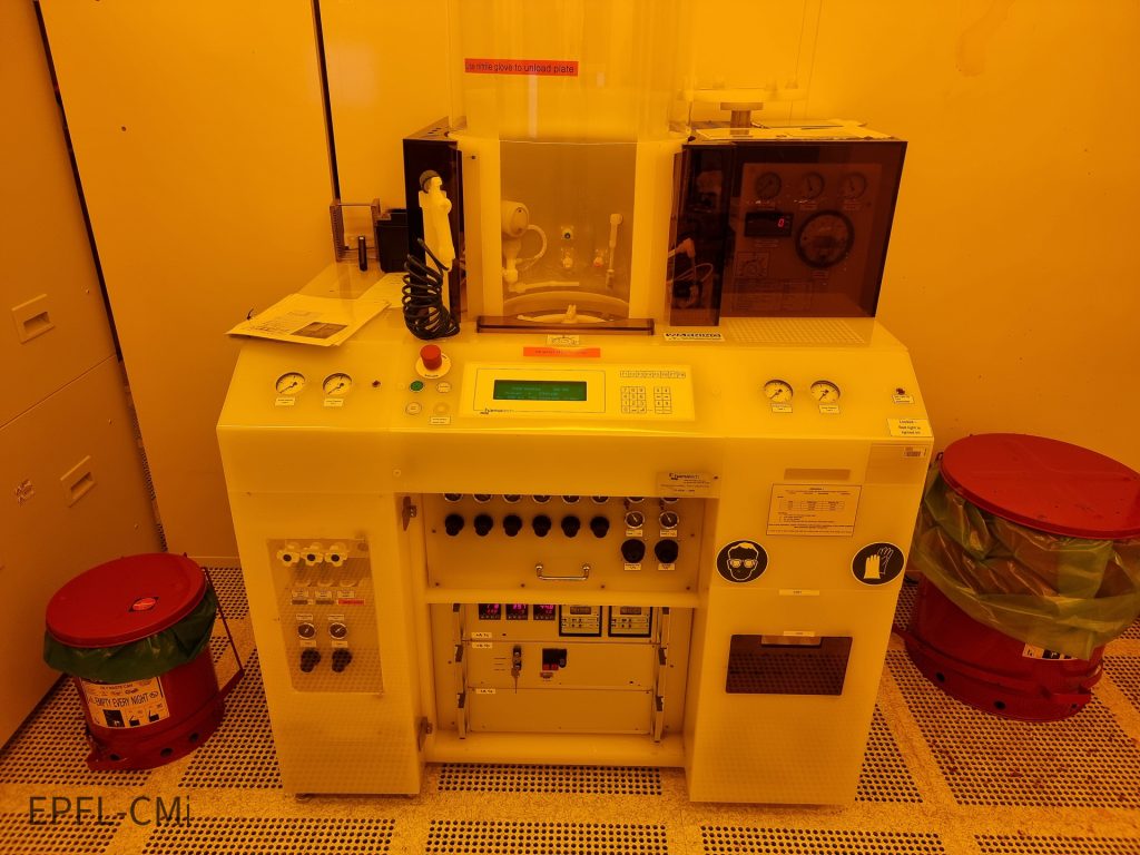
– Automatic (batch) spin-coating and development – 100mm and 150mm wafers – Maximum substrate thickness ~ 750um – Up to 9 photoresist pump dispense lines + 3 N2 pressure dispense lines – 3 photoresist developer lines (spray or puddle) – HMDS vapor-prime module – Effective mini-environment and temperature control in spin-modules
– i-line resists: AZ ECI 3007, AZ 3027, AZ 1512, AZ nLOF 2020, AZ nLOF 2070 – Protection resist: AZ P4K-AP – Lift-off bottom layer: LOR 5A, LOR 15C – Anti-reflection bottom layer (BARC): XHRiC-16 – Developer chemistry: AZ 726 MIF (2.38% TMAH), AZ Developer (aluminum firendly)
– Automatic (batch) spin-coating and development – 100mm and 150mm wafers – Maximum substrate thickness ~ 750um – Up to 7 photoresist dispense lines + 1 syringe line – 2 photoresist developer lines (spray or puddle) – HMDS vapor-prime module
– i-line resists: AZ ECI 3007, AZ 3027, AZ 10XT-20, AZ 10XT-60, AZ 40XT, AZ 15nXT – Developer chemistry: AZ 726 MIF (2.38% TMAH), AZ 400 K / H2O 1:3.5 (KOH)
– Automatic processing of masks, i.e. chrome blanks (Cr: ~100nm (LRC), PR: AZ1505 500nm) – Compatible with 4inch, 5inch, 6inch and 7inch plates – Photoresist development, chrome etch, photoresist strip steps are run in sequence or individually.
– Programmable spin-sequence for i-line photoresists – Sawatec SM-200 coater + SSE VB20 HMDS vapor prime module – 1 x high precision Präzitherm hotplate – 1 x high temperature hotplate – Chucks for wafers up to 200mm – Chucks for small chips (min. 10x10mm2) – Manual dispense
– Programmable spin-sequence for SU-8 – Combi coater + 2 x HP-200 hotplates – Chucks for 50mm and 100mm wafers – Chucks for small chips (min. 10x10mm2) – Manual dispense
– Programmable spin-sequence for polymers – 2 x high precision Präzitherm hotplates – Chucks for 100mm wafers and small chips (min. 10x10mm2) – Manual dispense
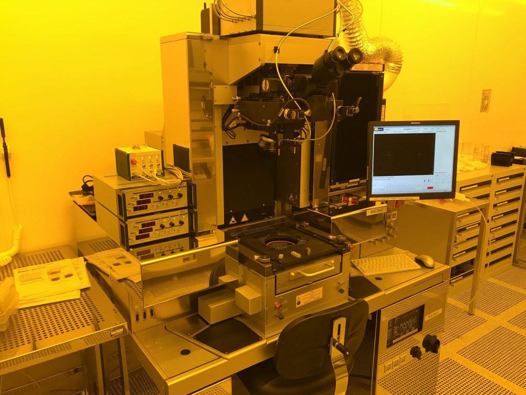
– Exposure with top-side or back-side alignment – Configurable Hg lamp illumination (i-line, g-line, broadband, DUV) – Multiple wafer/chip sizes up to 150mm wafer – Minimum wafer thickness ~ 200um (D263T glass wafers should be exposed on the EVG 610)
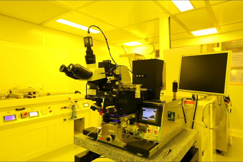
– Exposure with top-side alignment – i-line illumination (365nm) – Multiple wafer/chip sizes up to 100mm wafer – Holders for Cr masks and transparent foils – Dedicated chuck and objectives for chips
– Direct writing on Cr-blanks (4×4″ | 5×5″ | 6×6″ | 7×7″) or wafers (100mm | 150 mm). – Batch processing. Cassette to cassette. – UV-light source (i-line λ = 355nm) – Wizard for single or batch processing – Wizard for dose/focus calibrations – Advance mode for top side alignment overlay exposure – Compatible with .gds and .cif formats
– Direct writing on wafers and chips – Two laser sources (λ=405nm & λ=375nm) – Top- and backside alignment – Wizard for dose/focus calibrations – Compatible with .gds and .cif formats
– Direct writing on wafers and chips – Two laser sources (λ=405nm & λ=375nm) – Top- and backside alignment – Wizard for dose/focus calibrations – Compatible with .gds and .cif formats
– Thermal NIL up to 250°C – UV NIL @365nm or 405nm (with temperature up to 200°C) – Imprint in vacuum (~1mbar) – Uniform pressure (up to 6.5bar) applied trough a membrane – Replicable structures : ~40nm up to 100um
– Wet bench for solvent chemistry with beakers – Various beaker sizes and substrate holders – Solvents : acetone, IPA, PGMEA, TechniStrip Ni555 – DI H2O sinks with spray showers – 2x Bain-Marie with heating and ultrasonic options
– Wet bench for bases (developers) with beakers – Various beaker sizes and substrate holders – Bases: AZ 400K, AZ 351 B, AZ 726 MIF, AZ developer, TechniStrip P1316 – DI H2O sinks with spray showers – Centralized waste
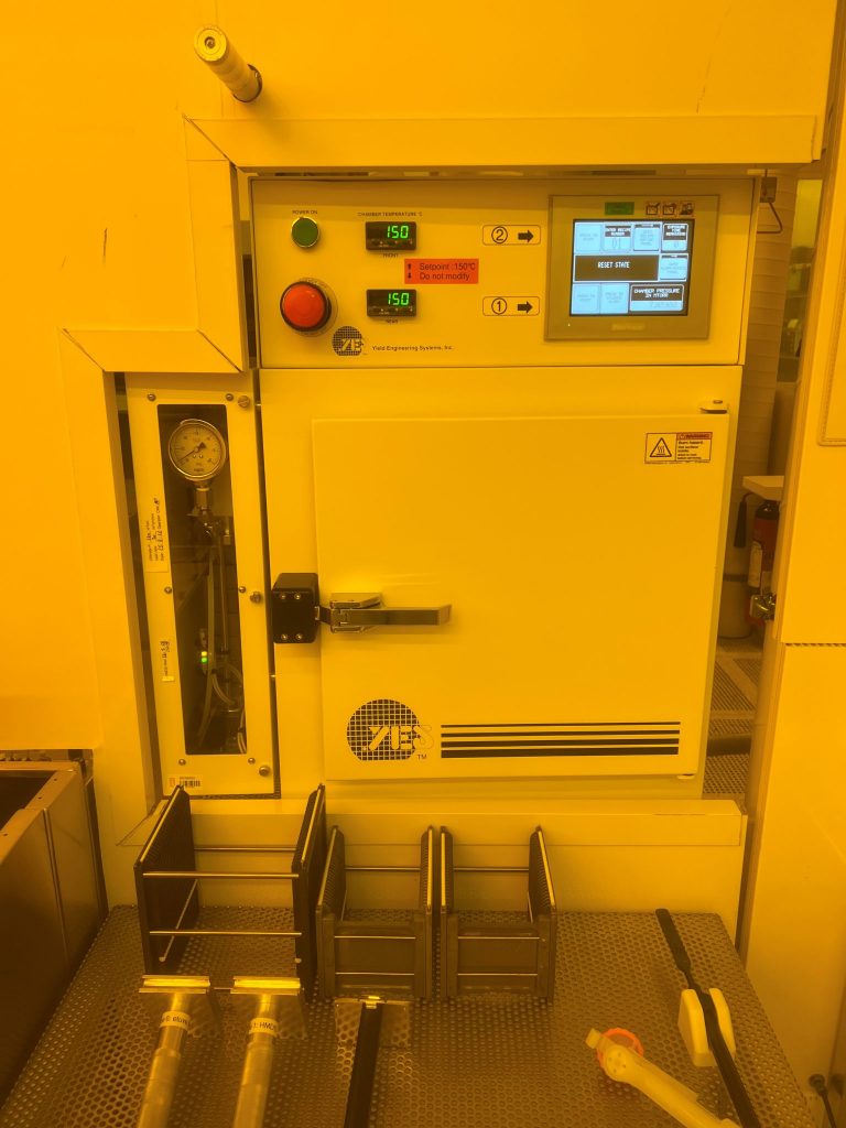
– Ovens dedicated to the hardbake of photoresists (overnight @ 85°C) – Maximum temperature: 300°C – Carriers for 100mm and 150mm wafers – Piece parts allowed
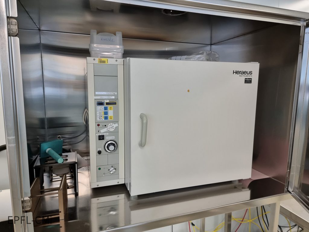
– Oven dedicated to polyimide full curing – Maximum temperature: 300°C – Carriers for 100mm and 150mm wafers – Piece parts allowed – Nitrogen circulation
– Only for biocompatible devices – Maximum temperature: 350°C – Carriers for 100mm and 150mm wafers – Piece parts allowed – Nitrogen circulation – High efficiency particulate air filter – Possibility to monitor temperature