Restrictions and Precautions
Materials such as pyrex, floatglass or any “fancy” metal (Cu, Cr, Au, Fe, Ag…) require CMi staff agreement BEFOREHAND
1. Maximum allowed booking per person between 9am and 5pm is 2 hours. It is still possible to get 4 consecutive hours from 7am to 11am or from 3pm to 7pm.
2. Reservation names must correspond to operators.
Contents
I. Introduction
STS Multiplex ICP offers large range materials etching possibility: insulators (SiO2, Si3N4 and SiC), silicon, metals (Al Alloys, Pt, Ti) and some polymers… At CMI, this etcher is dedicated for etching:
- metals (processes under chlorine chemistry)
- quartz (fluorine/carbonate chemistry)
- polyimide (oxygen chemistry)
Technological advantages of this equipment are the followings:
- High density plasma of ICP (Inductively Coupled Plasma ) type
- An electrostatic clamping and biasing chuck controlled in temperature (20°C) and adaptable for 4 inches and 6 inches wafers
- Powerful pumping systems
The major advantages of this system compared to capacitive coupled reactors (also called RIE: Reactive Ion Etching) are:
- Wafer voltage biasing independent from the inductively coupled plasma creation
- Creation of a low pressure (0.1 à 20 Pa) and high density (1011 à 1012 cm-3) plasma without reactor walls sputtering
This dissociation between the plasma density (radicals and ions) and the ions energy offers large processes development opportunities.
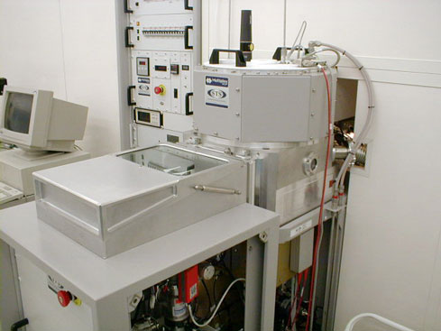
II. Equipment description
Graphic user interface
STS Multiplex ICP etcher is entirely computer controlled. The only manual handling is loading/unloading step of the wafers into the loadlock.
Transfer loadlock
The loadlock/transfer arm system is designed in such a way that the process chamber is always under high vacuum during loadings/unloadings procedures of the wafers, which optimizes processes durations.
Processing chamber
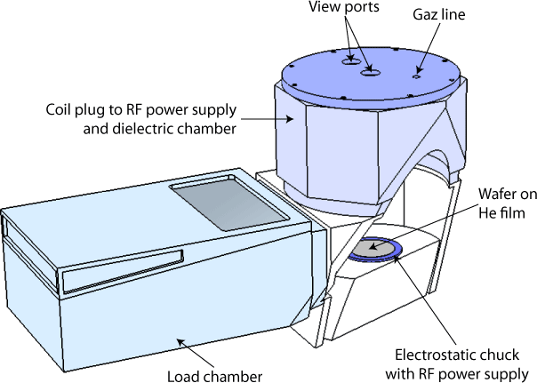
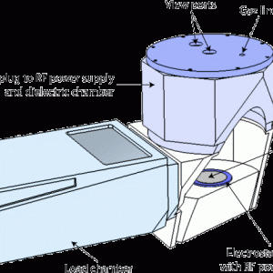
Figure 1 depicts a global view of STS reactor. Main parts are visible: ICP source, diffusion chamber, electrostatic and biasing substrate holder, pumping systems and gas lines. The machine is also fitted with an End Point Detection (EPD) system.
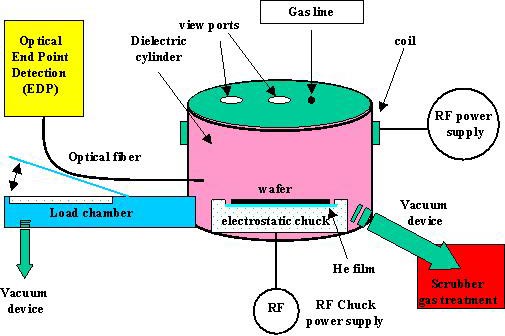
ICP source
ICP source is made with an antenna connected to an RF power supply and wrapped around an alumina cylinder. RF power is coupled to the plasma through an inductive mode. The oscillating current in the antenna at 13.56 MHz induces an electromagnetic field (E/B) in the alumina cylinder. For plasma ignition, some primary electrons collect the E/B field energy (ions are too heavy to get the energy from E/B field). Inelastic collisions between hot electrons and neutrals (injected gas mixture) give ions/electrons pairs. This is the way how the main plasma is created inside the cylinder where the gas mixture and pressure are controlled (turbo pump associated to a rough primary pump).
Electrostatic and biasing substrate holder
The electrostatic chuck (ESC) allows holding and thermalizing 100mm wafers to room temperature. Temperature control is assured by circulation of a thermostat liquid. The wafer, whose backside must be conductive, is fixed to the chuck by electrostatic clamping. Energy transfers between the thermalized chuck and the wafer is assured by a helium film whose pressure is adjustable. The substrate holder biasing is done by a RF generator (300 W maximum), which enables control of the ions mean energy value during the etching process.
Pumping systems
The combination of a 1000 l/s turbo pump and a rough primary pump gives a secondary vacuum of few 10-7 mb without process. In process, the powerful pumping capacity makes possible the use of high gas flow (to enhance etch rate) at a low pressure (few Pa). A secondary rough primary pump is fitted to the machine for load lock pumping.
Gas lines
Injection of gas mixtures is assured by 8 Mass Flow Controllers (MFC) for the following gas : O2 (100sccm), O2 (10sccm), SF6, CF4, BCl3, Ar, Cl2 and HBr.
These MFC can be used in pulsed mode with very low response times.
Gas treatment before drainage
Downstream the pumping system, outlet gases are treated before being drained. A M150 Gas reactor column from EDWARDS collects toxic compounds such as chlorine or fluorine through absorption in a cartridge tank heated between 450°C and 550°C.
III. Standard processes at CMi
| Material to etch | Process name | Mask | Selectivity/Mask | Etch rate (um/min) | Chemistry |
| Al | Al_etch | PR | >1:1 | 0.2 to 0.5 Si: 0.215 SiO2: 0.08 | Cl2/BCl3 |
| Diamond | Diamond | SiO2 | >2:1 | 0.08 | O2/Ar |
| Polyimide | Pyralin | SiO2 | >>50:1 | >>1 | O2 |
| Pt | Pt_etch | PR | 1:8 | 0.035 | Cl2/Ar |
| Si | Sub_Si | PR SiO2 | >1:1 8:1 | 0.35 | Cl2 |
| Si* | HBr_Si* | PR SiO2 | 2:1 >>50:1 | 0.2 | HBr/O2 |
| Si3N4 | Nitrure | PR | 1:1 | 0.2 | CF4 |
| SiO2 | Oxide | PR | 1:1 | 0.25 | CF4 |
| Ta | Ta_CF4 | PR | 1:1 | 0.1 | CF4 |
| Ti | Ti_etch | PR | 1:1 | 0.2 | Cl2/BCl3 |
| TiN | TiN_etch | PR | > 1:1 | 0.2 | Cl2/BCl3 |
| W | W_etch | PR | > 1:1 | 0.5 | SF6 |
| AlN | -AlN | SiO2 | 4:1 | 0.3 (sputtered) 0.17 (epitaxial) Mo / Pt: 0.037 | Cl2/Ar |
| Al2O3 | -Saphir | PR SiO2 | 0.05 (ALD) 0.09 (sputtered) | Cl2/BCl3/Ar |
*: silicon etch with HBr_Si process requires chamber priming and test wafer process before processing. It takes between 1 and 2 hours extra time to prepare the tool.
Reminder:
Some manual adjustments are needed for the Oxide recipe and the Pyralin recipe:
- Check the process parameters before starting the etching (IV. How to use the system – Step 11).
- Start the process.
- Move to Platen / Coil RF Power fields by using arrows of the keyboard.
- Modify values and validate with ENTER.
- Do so as quickly as possible.
IV. How to use the system
Starting situation:
- The machine is ON
- The screen of the PC is turned off
- The pump of the load-lock is stopped
- The ionic gauge is not under tension
- The loadlock is closed and vacuumed
- Login to the PC in Zone 2
- Turn on the monitor of the computer of the STS machine
- Start the load-lock pumping by actuating flip up CB5 which is at the right side of the uppermost electronic rack placed on the left engine
- On the screen C:\EPFL is seen: Type PROCESS, press ENTER
- Choose the desired program and press ENTER
- Wait until the message PROCESS LOADED OK appears at the lower right part of the screen
- Press the key F3 (load/unload), the page of the load-lock appears
- A menu, whose functions can be activated and are written in yellow, appears. Type V (vent load lock). This function lasts approximately 3 minutes and brings the load-lock to atmospheric pressure
- Open the lid of the load-lock, place a substrate (etching surface up), close the lid
- Type L (load wafer). This function lasts approximately 2 minutes, and transferred the wafer into the etching chamber. Press F3 to leave the page of the load-lock
- The substrate is in place on the substrate carrier, inside the etching chamber. The preselected-process (selected at step (5)) can be started by directly pressing F1 (etch). However, it is advised to check the process parameters before starting the etching according to the following procedure:
- Press F6 (main menu), the main menu is activated. Type LEVEL
- Press ENTER. The password required is PROcESS (respect the c small-letter). A new list of headings is proposed
- Type SETUP and press ENTER
- Using the arrows keys, select the column LOAD/SAVE/DEL, then select the line LOAD PROCESS and press ENTER
- Select your program and press ENTER
- Select the column ETCH DEF’ N, then the line MODIFY STEP and press ENTER 2 times
- To modify the etching time, select the heading “RF info”, then “Coil SETTINGS” and press ENTER
- Select PROCESS TIME, type ENTER and insert the time you want by respecting DOS syntax
- In the same way it is possible to modify the other parameters of the process
- Press ESC. And select the column LOAD/SAVE/DEL, then select the line SAVE PROCESS and press ENTER
- The software shows, by default, the name of the program which has been selected at step (5), press ENTER
- A warning message appears, that informs you a program already exists with this name. To overwrite type Y, then, 2 times ESC, and Y again
- Press F8, then press F1 to start etching
- While plasma is starting, check that the substrate is correctly clamped on the substrate carrier (without any vibration). If the substrate is vibrating then it may quickly heat-up which may damage and destruct the photoresist mask. So, in case of any vibration, the following procedure should be followed:
- Press F1 (Abort) Immediately. The etching program is stopped
- Then press F3, then unload the substrate (Unload then Vent)
- Open the load-lock and replace correctly the substrate on the transfer arm
- On the bottom track of STS power supply (left of machine) , locate the connector block UNCLAMP and press the white button PUSH TO RESET. A pneumatic noise heard, the electrostatic clamping device is reinitialized
- Return to the processing bay (front of the machine), reload the substrate, press F3 and start the etching program again by pressing F1
- When the process is finished, PROCESS ENDED OK appears in the right lower portion of the screen
- Press F3 (load/unload), the page of the load-lock appears
- Press U (unload wafer). The transfer arm will transfer the etched substrate to the load-lock
- Press V (vent load lock) to ventilate the load-lock
- Open the load-lock, discharge the etched substrate and to continue either by etching a new substrate (return to step (9)), or put the machine to the idle mode with the following procedure:
- Press F3, then without putting any wafer onto the transfer arm, press L (Load)
- Press U (unload), so the load-lock is vacuumed
- Type F3, then F4 (Shut Down) and turn the switch CB5 OFF
- Turn off the computer monitor and logout from the PC at Zone 2.
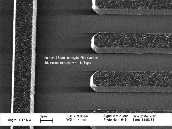
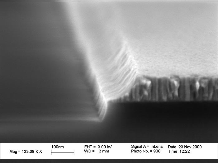
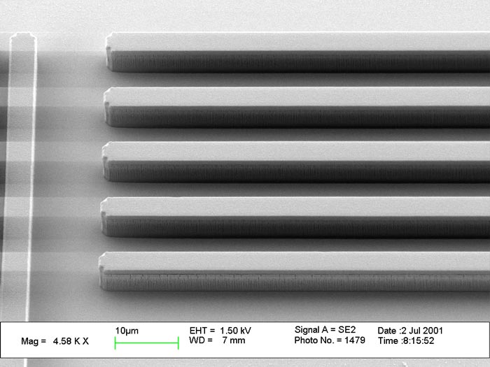
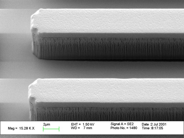
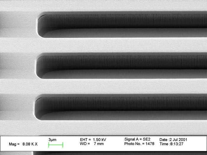
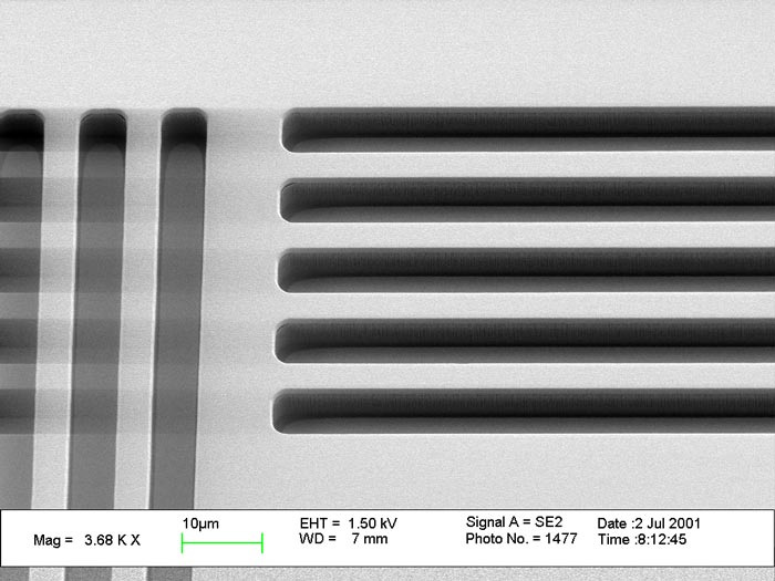
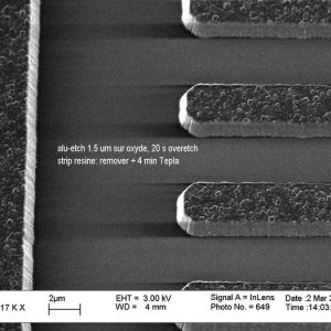
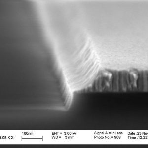
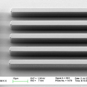
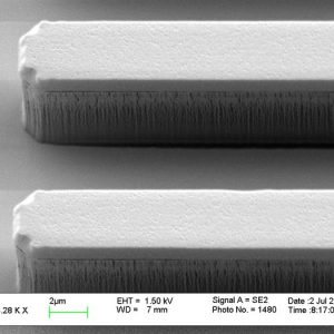
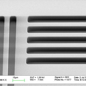
V. Photos gallery