In general, it is recommended to perform photolithography (and all microfabrication steps) at the wafer-scale. Most of the automatic photolithography equipment (Süss ACS 200, EVG 150, TEL ACT 8, ASML PAS 5500/350C, HIMT VPG 200) are compatible only with 100mm (or 150mm) SEMI wafers.
However, in CMi, several equipment can be configured and used to perform photolithography on small rectangle-shape substrates (chips), which are typically diced from 100mm wafers.
Users working with chips will use the following tools to perform the photolithography steps:
- Photoresist coating: Sawatec SM-200 manual spin-coating equipment in Zone 13.
- Photoresist exposure: Heidelberg Instruments MLA-150 direct laser writing equipment in Zone 16.
- Photoresist development: Arias base wet bench in Zone 13.
On these equipment, small substrates can be handled directly as a chip or glued on a 100mm silicon carrier wafer using the QuickStick 135 temporary wax for easier manipulation and compatibility with other microfabrication equipment (automatic coater/developper, etching and thin film deposition tools).
Nonethless there are technical limitations with the tool operation and capabilities that limits the size to a minimum. These limitations are detailed in the gallery below.
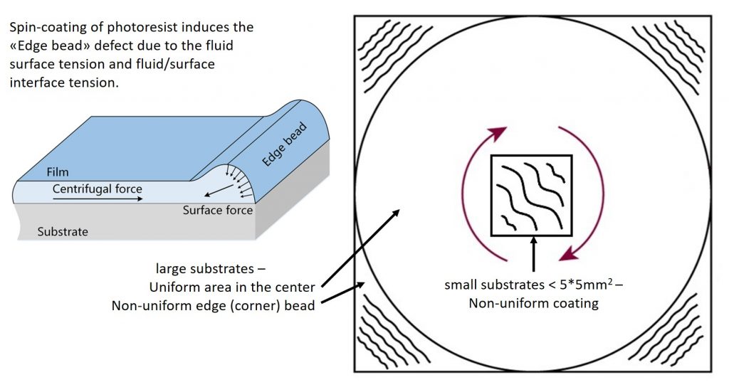
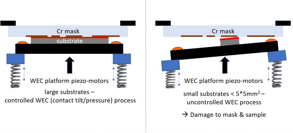
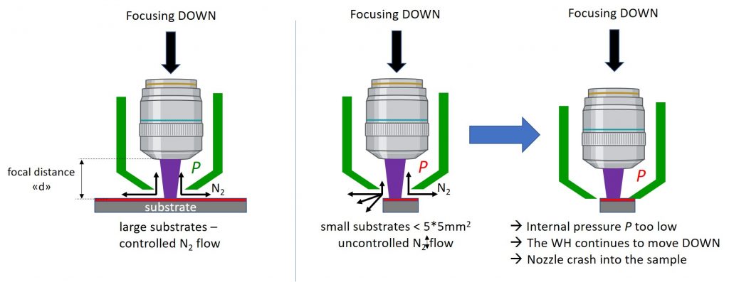
! The minimum sample size that can be used on these tools without additional precautions is 5mm * 5mm !
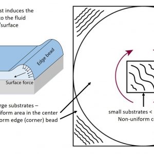
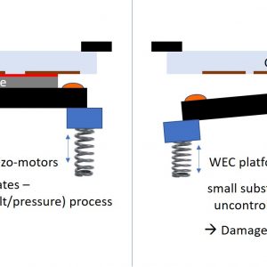
Using samples with dimensions less than 5mm * 5mm, you will not be able to obtain stable and reproducible exposure results, you may damage your samples and, worse, you may damage the CMi processing equipment, resulting in several costly hours of downtime for repair and calibration.

Acceptable work-around solutions fo chips < 5mm * 5mm
In the case where the users strictly have no choice but to use samples with dimensions less than 5mm * 5mm, then the following two options should be considered:
- Using a 100m silicon wafer with pockets to fit in small samples.
- Using a 100m silicon wafer as a carrier for several packed samples covering an area > 5mm * 5mm.
! Please note that the use of samples with dimensions less than 5mm * 5mm should be imperatively communicated to the CMi staff by sending an update of the user’s active process flows to [email protected] !
! In addition, the first use of the work-around solutions on the photolithography equipment should be done with the CMi staff assistance as some additionnal precautions or options might be necessary to achieve good results and guarantee the safe operation of the tool !
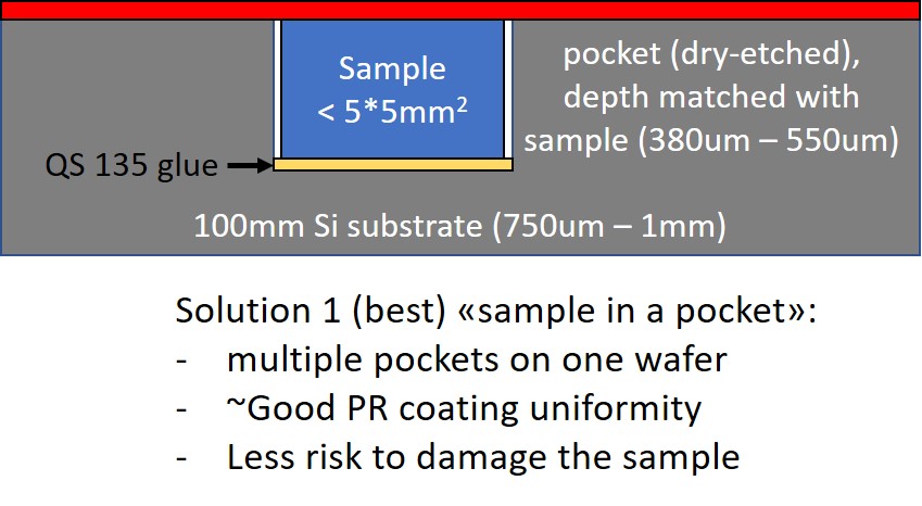
Solution 1: Fabrication of a silicon wafer with pockets
A thick silicon wafer can be patterned by standard photolithography using a thick photoresist such as AZ-10XT 60, or, alternatively, with a SiO2 hardmask, and further etched into silicon using deep RIE etching (Bosch process) to create pockets slightly larger than the sample dimension (by a few hundreds of microns). Users should try to match the depth of the pockets with the thickness of the sample as accurately as possible.
Multiple pockets can be created on a single wafer to fit several samples that will be exposed one after the other on the MLA 150 direct laser writer.
The same strategy can also be used to expose with a mask-aligner but with only one pocket located at the exact center of the wafer.
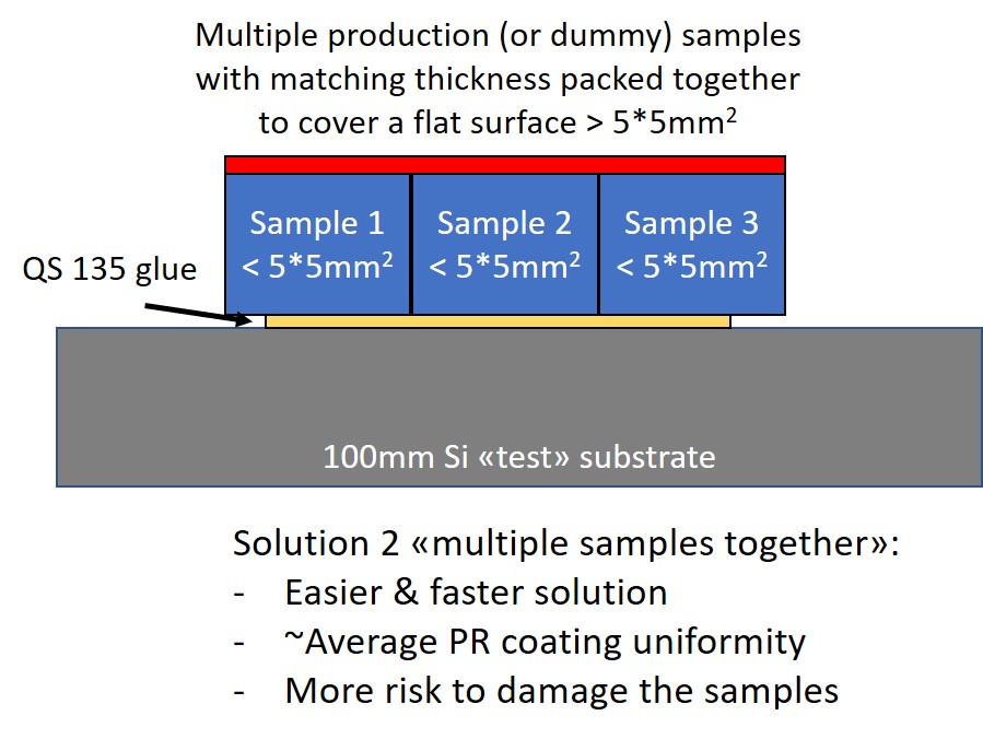
Solution 2: Using a silicon carrier wafer with closely-packed small samples
A standard silicon wafer can be used as a carrier for several of the user’s chips (instead of one). Samples (production or dummy) with matching thickness should be placed and glued (with QS 135) closed to each other in a fine arrangment so that the overall surface is flat over a distance of more than 5mm * 5mm.
This approach is easier to implement than solution 1 but the PR coating quality will be significantly worse and there are more risk to damage the samples.