Please use the Service request interface to make a grinding request.
Contents
- Introduction
- Grinding mechanism
- Equipment description
- Associated equipment
- Grinding capabilities at CMi
- How to use the system
I. Introduction
The DAG810 is a compact, automatic grinder for silicon, III/V materials (GaN, GaAs, InP…) and various glass types (pure amorphous SiO2, float glass, pyrex…). It is used to thin down single wafers, stacked wafers or chips of any shapes and dimensions (from a few mm2 to full 8″ wafer). Grinding speed as high as 30microns/min is achievable with a total thickness variation (TTV) close to one micron, and a surface roughness less than 100nm.
II. Grinding mechanism
The workpieces are clamped to a rotating chuck table, across the center of which a rotating diamond wheel sweeps. The spindle carrying the wheel moves downward to remove the material from the surface of the workpieces. Water is used to cool the workpieces and to clear particles and mud generated during grinding. Fine control of the spindle vertical displacement, as well as precise angular adjustments with the chuck table, give a flat ground surface with a TTV of ~1um.
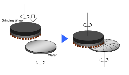
The thickness reduction is accomplished in 2 or 3 different phases to ensure low-load grinding. This is done by decreasing the feed speed (um/s) of the grinding wheel as finishing thickness is closed.
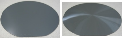
Wafers edges initially show a rounded shape, but when being ground, these edges take on a sharp shape and mechanical strength is weakened. Because of the cooling water and the grinding conditions, this weakened edge area may induce breakage (depending of the final thickness).
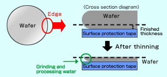
Accelerating at the chuck table rotation speed, while decelerating at the spindle rotation speed, prevents the edge area from being damaged (no edge chipping).
After grinding, the surface of the workpieces is always damaged and this can be divided into different zones. The first one reveals the roughness linked to the wheel being used (coarse wheel, fine wheel or even polygrind wheel for ultra-thin finishing). The second zone, a layer typically in the range of 2um to 10um thick, is full of micro-cracks, which causes stress in the workpieces. Then, a zone of crystal dislocations is present before recovering the typical arrangement of the material.
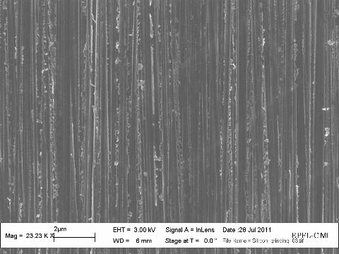
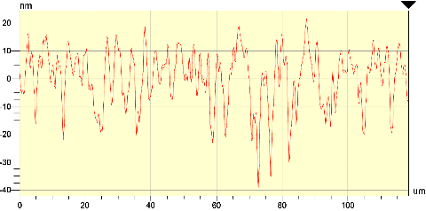
Root-mean-square roughness Rq ~10nm
Max peak-to-valley difference Ry ~60nm
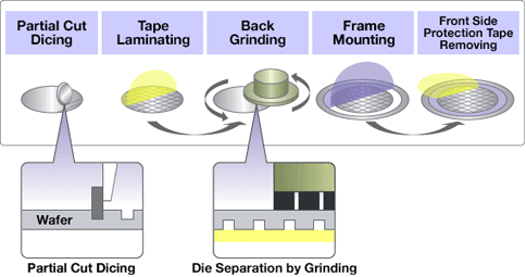
The surface roughness can be reduced and the stress induced by the micro-cracks can be released by removing few microns of material using dry or wet etching or polishing techniques. Stress relief on the edges of chips can also be performed by doing a Dicing Before Grinding (DBG): dies are separated by grinding after half-cutting the workpieces.
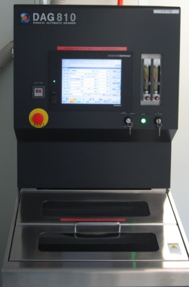
III. Equipment description
The equipment is composed of:
- One universal vacuum chuck table for 4″, 5″, 6″ and 8″ wafer size
- One mechanical frame clamping for UV-tape mounted wafers or chips
- One high-rigidity, low-vibration spindle to achieve superior grinding result
- Dedicated grinding wheels according to material, grinding speed and final roughness to reach:
– Coarse and fine silicon grinding (2 different wheels)
– Coarse and fine glass types grinding (2 different wheels)
– GaN fine grinding (1 wheel) - Real-time probe-height from 4″ wafer size
- LCD touch screen for easy and intuitive operation
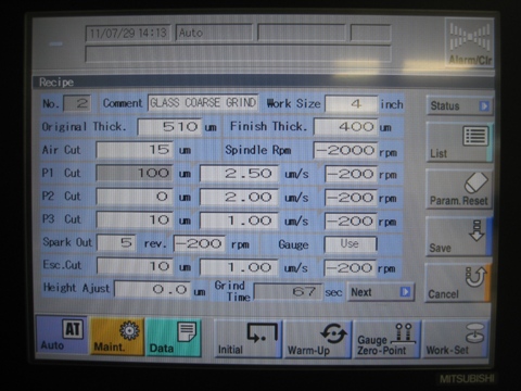
The equipment is software-driven but some manual operations are requested for each grinding:
- Selection and installation of the correct wheel
- Axis initialization and machine warm-up (only at machine starting)
- Probe-height initialization (if being used)
Note: Probe-height is not usable with chips, wafers with topography and wafers smaller than 4″ (Risk of damage/breakage) - Wafer thickness measurement before and after grinding (manual prober)
- Workpieces loading and unloading
- UV-tape mounting, cleaning and curing if needed
IV. Associated equipment
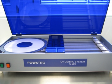
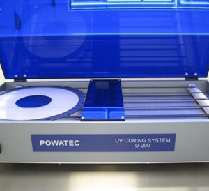
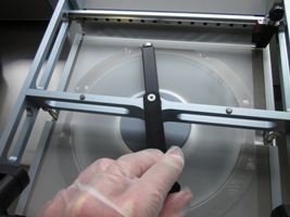
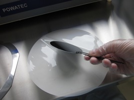
Dedicated frames are available to ensure perfect handling and cleaning of the workpieces. They are used in combination with a UV sensitive tape to handle chips or even wafers (Powatec Wafer Mounter P-200). After grinding, the Automatic Cleaner DCS1440 gives clean and dry workpieces that are then safely released when exposing the tape to UV light (Powatec UV Curing U-200).
Powatec Wafer Mounter P-200 and UV Curing U-200
Manual is available HERE.
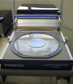
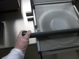
The P-200 from Powatec is a manual wafer mounter fitted with dedicated frames, cutter devices and pad roller enabling bubble free mounted wafers or chips onto UV-sensitive tape.

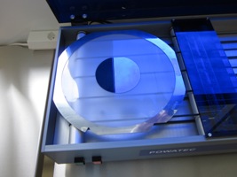
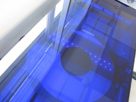
The U-200 from Powatec is a manual UV irradiation system fitted with 31 LED’s (310mW @ 365nm). It is used to cure UV-tape to ensure easy and safe removal of thin workpieces.
Manual is available HERE.
Cleaner DCS1440
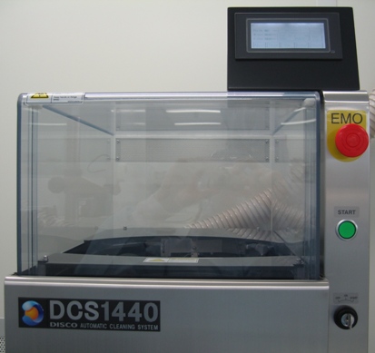
The DCS1440 is used to clean and dry workpieces handled on frames + UV-tape. Mist generated by mixing fluid droplets with blasts of air is sprayed against the cleaning surface at high speeds (atomizing cleaning). The workpieces are then dried by fast spinning + air blow. Document from DISCO is available HERE.
V. Grinding capabilities at CMi
The DAG810 has been tested for the followings:
On single wafers
- Silicon wafers:
– 100mm diameter, 525um reduced to 100um
– 150mm diameter, 625um reduced to 200um - GaN 2″ wafer (mounted on frame), 320um reduced to 100um
- Fused silica wafer, 525um reduced to 200um
- Pyrex wafer (borosilicate), 525um reduced to 200um
- Glass wafer (sodalime), 525um reduced to 200um
On stacked wafers
- Pyrex/Si anodic bonding, Si thinning down to 30um
- Si/Si wafers mounted with quickstick 135, Si thinning down to 50um
- Si/glass wafers bonded with parylene, Si thinning down to 50um
- Si/Si wafers mounted with spined glue, Si thinning down to 50um
Chips on UV-tape
- GaN 2cmX2cm, 320um reduced to 100um
- Silicon 1cmx1cm, 380um thinning down to 50um
- Smaller Si chips (few mm), 380um thinning down to 50um
- Fused silica 1cmx1cm, 380um thinning down to 50um
- Pyrex 1cmx1cm, 380um thinning down to 50um
VI. How to use the system
For now, grinding is done as a service by CMi staff. Grinding request here.