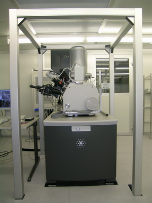
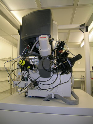

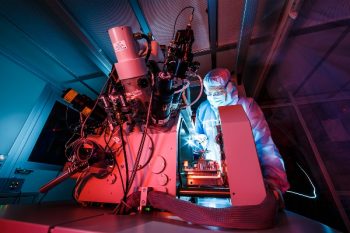
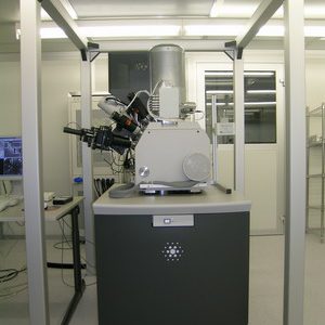
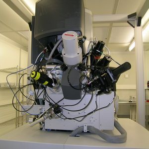
The Nova 600 NanoLab is a Dual Beam SEM / FIB for nanoscale prototyping, machining, characterization and analysis. It combines ultra-high resolution field emission Scanning Electron Microscopy (SEM) and precise Focused Ion Beam (FIB) etch and deposition.
Contents
- Description
- Machining performances
- Hardware, software and holders options
- Preliminary operations
- Cross-sections – TEM lamellas
- Pictures and misc
I. Description
-
Geometry
On a 21-port specimen chamber the electron and ion column are mounted at 52 degrees to each other. The beam coincidence point is at 5 mm working distance, which is also the eucentric working distance of the stage and the analytical working distance.
-
Vacuum
The Nova 600 NanoLab uses a vacuum system, which is entirely oil-free. Differential pumping on the electron column ensures tip operation at the ultra-high vacuum levels (10-10 mbar) even with a controlled gas flow in the specimen chamber.
-
Sample navigation
The Nova 600 NanoLab is equipped with a 5-axes motorized x-y-z-rotate-tilt stage. Travel along the x and y-axis is 150 mm, the tilt range is –5 to 60 degrees. The motorized z-range is 10 mm. Minimum step size is 100 nm, repeatability at 0 degrees tilt is 1 µm, and 2 µm at 52 degrees tilt.
-
Detection
The Nova 600 NanoLab features in-lens SE and BSE detection for high-resolution imaging at both high and low kV’s, as well as an Everhart-Thornley SE detector for conventional SE detection. Optionally available is a 2-segment solid-state STEM detector for both bright- and dark-field imaging and Nano-analysis of FIB-prepared cross-sections. An integrated IR-CCD camera is standard for in-chamber viewing.
-
Imaging
Images are displayed in an area of 1024 x 884 pixels, configurable for single frame display or 4-quadrant display. Images can be viewed live, averaged or integrated. Images can be saved in TIFF, BMP or JPEG file formats, and in 8-bit or 16-bit depth, to the hard disk or LAN from the graphical user interface. Image printing is also available from the user interface.
-
Patterning
Predefined patterns can be drawn in overlay in any of the four quadrants in the User Interface. Progress of the patterning is monitored in the User Interface through a progress bar. End-point detection is available through an integrated Real-time monitor. Simultaneous imaging and patterning is a standard feature of the Nova 600 NanoLab.
-
Electron optics
Magnetic immersion lens electron optics with ultra-high brightness Sirion emitter:
-
- Source: Schottky field emitter, Sirion type.
- Source lifetime: 1 year guaranteed.
- Voltage: 200 V to 30 kV, continuously adjustable.
- Beam current: < 20 nA.
- Resolution: 1.1 nm @ 15 kV, 2.5 nm @ 1 kV (< 60 dBC).
- Detection: in-lens secondary electrons (SE) and back scattered electrons (BSE).
-
Ions optics
Magnum™ field emission focused ion beam optics (liquid Gallium ion emitter):
-
- Source lifetime: 1500 hours.
- Voltage: 5 kV to 30 kV.
- Beam current: 20 nA in 15 steps.
- Resolution: 7.0 nm @ 30 kV.
- Detection: CDEM detector (direct ion detector).
-
Scanning System
High-resolution digital scanning engine controlled from the User Interface:
- Resolution: 512 x 442, 1024 x 884, 2048 x 1768, 3584 x 3094 pixels.
- Minimum Dwell Time: 50 ns / pixel.
- Electronic scan rotation by n x 360 degrees
-
Patterning System
High-resolution digital patterning engine controlled from the User Interface:
-
- Maximum resolution: 4k x 4k x 8 bit.
- Minimum Dwell Time: 100 ns / pixel.
- Maximum Dwell Time: 4 ms / pixel.
- Multiple pattern shapes.
- Variable dwell time pattern to give 3D milling.
- Complex milling patterns through Bitmap import.
II. Machining performances
-
Machining performances
- Minimum deposited line width : 20 nm achievable with electrons and 50 nm achievable with ions beam (Pt).
- Minimum etched line width: < 15 nm achievable (Si).
- Maximum hole aspect ratio: 10:1 (Si, 500 nm hole radius).
- Typical TEM sample thickness: 50-100 nm (30-50 nm achievable).
-
Fabrication
- Predefined patterns (line, rectangle, polygon, circle, ring, regular cross-section and cleaning cross-section). Predefined patterns can be drawn in overlay in any of the four quadrants in the User Interface.
- Bitmaps. 24 bit bitmaps can be imported.
- Stream files. Stream files are ASCII or binary files that contain the screen locations of each point to be milled.
- Script files. A script file is a list of commands that can be executed without user interaction.
- 1 M pixels addressable.
III. Hardware, software and holders options
-
Insulator deposition
Gas chemistry (TEOS) solution for in-situ deposition of insulator material, preferably mounted on GIS port 4. The resistivity of the deposition has been greatly improved with this release of Insulator deposition which includes an additional deposition enhancement gas. -
Platinum deposition
Gas chemistry solution for Ion or Electron beam deposition of Platinum-containing material. Platinum gas chemistry is the preferred metal deposition in case ease of use, high deposition rate and precision of the deposition is required. -
Insulator enhanced etch
Gas chemistry solution (XeF2) for enhanced etching of insulator materials, mounted on any of the available GIS ports. This gas chemistry is used to selectively remove insulating materials while inhibiting the removal of conducting materials. -
Selective carbon mill
Gas chemistry solution for enhanced etching of polymer-based materials such as resist, polycarbonate or diamonds. It mounts on any of the available GIS ports.
-
Omniprobe system
The Omniprobe is FEI’s preferred solution for in-situ TEM sample lift-out. -
Electrostatic beam blanker
The Electrostatic Beam Blanker is an essential tool for Lithography applications on SEM and Small Dual Beam. This option will blank the Electron Beam with a decay/rise time of 1 ns when an external blanking voltage of +8 V is applied. The E-Beam will pass the column undisturbed when a voltage of 0 V is applied. -
Solid-state STEM detector
Two-segment solid-state STEM detector for high-resolution bright and dark field imaging of FIB-prepared cross sections and critical dimension measurements. The STEM detector is designed to hold up to 6 FIB-prepared sections placed on copper-grid supported carbon film. -
CDEM detector
Channel Detection Electron Multiplier (CDEM) for direct ion imaging and ion-induced secondary electron imaging. The geometry of the detector is optimized for imaging with the ion column resulting in excellent S/N in ion imaging, as opposed to the Everhart Thornley SED which is optimized for S/N in electron imaging. The CDEM detector can be used in combination with the charge neutralizer providing ion imaging while the specimen is flooded with electrons to neutralize charge.
-
AutoFIB
Multi-site, multi-task automation software for the Nova NanoLab. The software includes image recognition software. Application-specific automation software can be built on top of AutoFIB. AutoTEM is an example of such application specific software and hence requires AutoFIB. -
AutoTEM
Automation software for unattended TEM sample preparation by Focused Ion Beam Nano-machining. Throughput typically is two samples per hour depending on the required final thickness of the sample. The AutoTEM option requires Auto-FIB and Platinum or Tungsten gas chemistry. -
Auto slice and view
Automation software for unattended serial sectioning and imaging through a site-specific volume of the specimen. The sequence of images can be merged into a video or be used as the input for 3 dimensional reconstruction of the volume subjected to the slice and view process. -
Pro image analysis software
Extended Image Analysis Software Package including image archive, particle analysis, FFT and scripting capabilities.
-
UMB stub holder kit
Specimen stub holder kit containing the following items:- Universal mounting base (UMB).
- 2 stub modules each holding 3 ½ inch stubs 2 or 1 inch stubs, 2 clamp bars.
- System calibration sample.
-
UMB FIB/TEM specimen holder kit
TEM specimen holder kit containing 2 row holders for 6 TEM samples each. Also included are 2 row holder carriers, a storage box and a sample loading base. FP 3660/00 UMB Stub holder kit is required for this option. -
Vise specimen holder
Clamp specimen holder to mount irregular, large or heavy specimens to the specimen stage. -
4” wafer holder (100 mm)
Light-weight, aluminium wafer holder for 4” wafer with flat. The holder is delivered with an aluminium protective case. An Allen key is required to mount the holder to the rotation platform of the specimen stage. -
6” wafer holder (150 mm)
Light-weight, aluminium wafer holder for 6” wafer with flat. The holder is delivered with an aluminium protective case. An Allen key is required to mount the holder to the rotation platform of the specimen stage.
IV. Preliminary operations
- Log on the main computer of the zone.
- On the tool computer, show or start the User Interface if it is not already.
- Log on the User Interface (File -> Log On).
- Vent the chamber with “Vent” button.
- Set the stage position at X = 75 mm, Y = 75 mm.
- When the chamber is vented, NEVER press on the stage or the door!!
- Load your sample with the appropriate holder.
- Close the chamber, start the pumping with “Pump” button and maintain the door of chamber properly closed.
- When the chamber is pumped, start the beams with the “Wake Up” button.
- Set the stage position at X = 0 mm, Y = 0 mm.
- Activate quad 1 and choose the electron beam as the active beam if not already selected.
- Click on the “(un)pause” button to begin scanning.
Note: Make sure e-beam parameters are in right conditions: detector ETD (Scan mode 1), 5kV or 10kV high voltage and ~100pA current. These are typical conditions to start with.
- Choose scanning parameters (speed, resolution, contrast, brightness…) that are comfortable to work with
- Also, start with zero beam shift: right click into “Beam Shift” and “zero”.
Tip: If very low contrast imaging or even no imaging, check e-beam emission is correclty aligned for the selected beam: activate “Crossover” option and make sure the “Source Tilt” is aligned with the green cross shown on quad. Deactivate “Crossover” option when done.
- Zoom in to about 5000X, adjust the focus on your sample and link the FWD (Focused Working Distance) to the Z-coordinate of the stage by clicking on the “Z=FWD” button.
Tip: You have to click on this button each time you change the focal distance because the system links the Z axis to the focal distance and not the reverse.
When working with the Dualbeam, setting the eucentric height is the most important part. At the eucentric point, the stage tilt axis, the ion and electron beams axes and ll of the Dualbeam components intersect.
At this point, and during stage tilt, the feature of interest stays focused and almost no image shift occurs.
- Set the stage Z-coordinate at 5 mm.
- Adjust the focus on your sample and again, link the FWD to the Z-coordinate of the stage by clicking on the “Z=FWD” button.
- Again, set the stage Z-coordinate at 5 mm.
BEFORE TILTING, and if possible, always rotate the stage (compucentric rotation) so on CCD camera view most of your sample is on the right side of the quad: most of the sample will “drop away” from the column when tilting; it is a safe position.
- Zoom in to about x10000 and center a recognizable horizontal target point (double click on it with the left mouse button).
- Tilt the T-coordinate of the stage to 7°;. Probably, the feature will shift during the stage move.
- Bring the feature back to the center of the quad by adjusting the stage Z-height: activate quad 3, choose the CCD view as the active view if not already selected, and use medium mouse button to drive the sample up or down.
- Tilt further to 52°; and again, acting into CCD view quad 3, bring the feature in the center of the screen.
- Tilt back to 0°;. The feature should not move significantly (max 5 to 10 microns).
- Tilt back to 52°; and final adjust the stage height if needed.
SEM
- Use the “Auto Contrast and Brightness” function (F9) if needed.
- Adjust the focus, the stigmatism with “Stigmator” and the lens alignment with the “Modulator” button and “Lens Alignment” setting. Loop through these three settings until you reach the needed resolution.
FIB
- Activate quad 2 and choose the ion beam as the active beam if not already selected.
- Select a beam with a low energy (eg. 30 kV, 30 pA).
- Clic on the “(un)pause” button to begin scanning.
- Use the “Auto Contrast and Brightness” function (F9).
- If needed, adjust the focus to 19.5 mm (distance at which beams are aligned) and the stigmatism with “Stigmator”.
- Take a picture (“snapshot” or “photography”, depend on needs)
- Freeze the image (= beam blanked) when done.
Tip: When scanning the sample, keep in mind than you can dramatically affect it with Ga+ ions. It depends on three parameters: the acceleration voltage, the beam current and the magnification. These parameters define the power density of the beam. The larger the beam density, the stronger the milling! So above a certain threshold, the sample is etched. Because of that, we advice you to pause the ion scanning as often as possible.
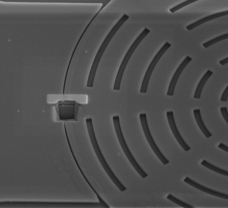
V. Cross-sections – TEM lamellas
If working with delicate substrate surfaces (e.g. stack of thin layers), it is recommended to deposit some Platinum surface protection with the electron beam first. This will avoid Ga+ ions damaging the surface in the initial phase of the preparation.
- In SEM mode 1, ETD imaging, use 2kV or 5kv,1nA range.
- Set the stage tilt at 0°, but at eucentric height!.
- Turn on the Pt GIS by a double click on “Cold”.
- When the Pt GIS is Warm, insert it.
- Define a rectangle pattern with dimensions typically 15µm x 2µm.
- Set the application to “Pt dep ebeam surface” or “Pt dep ebeam structure” (depends on presence of topography or not), and set a deposition time between 3mins to 5mins.
- When deposition is done, retract the GIS, set the ebeam back to normal imaging conditions, and tilt the sample back to 52°.
Thick protective Pt layer
-
- Turn on the Pt GIS by a double click on “Cold”.
- When the Pt GIS is Warm, insert it.
- On FIB quad 2, and over the area of interest, or over the e-beam deposited rectangle if that was used, deposit 1 to 3µm of Pt using the normal “Pt dep” application conditions.
The typical dimensions will be 15µm x 2µm. Typical current is 0.3nA. - When deposition is done, retract the GIS.
Main cut
-
- Switch to a high ion current, typicaly higher than 3nA.
- Define a “regular cross section” below the deposited strap of Pt. Typical dimensions are 20µm x 8µm, and a depth of 4µm. Make sure there is about 0.5µm between the upper edge of the regular cross section pattern and the lower edge of the deposited strap.
For cross-sections:
-
- With a 3nA beam, finalize by doing a narrow rectangle on top edge of the trenche, just touching the Pt strap.
Typical box size is 19µm x 1µm and a depth of 4µm. - Overlapping onto the Pt strap, then do a “cleaning cross section” to polish the sidewall of the cut.
- With a 3nA beam, finalize by doing a narrow rectangle on top edge of the trenche, just touching the Pt strap.
For TEM lamellas:
- Do the same main cut as above on the other side of the deposited strap, but rotate the regular cross section pattern by 180° to make sure the deep end is near the Pt strap!
- With a 3nA beam, finalize by doing a narrow rectangle on the edge of both trenches, just touching the Pt strap.
Typical box sizes are 19µm x 1µm and a depth of 4µm. - Change FIB current to 1 or 3 nA.
- Tilt the sample to 7°: the ion beam hits the lamella at 45°.
- In the FIB image, define 3 rectangle patterns and set to parallel milling:
- 1 horizontal near the bottom of the trench (~ 800 nm high).
- 1 vertical at the left side of the lamella (1 µm wide, height all the way over the top of the sample).
- 1 vertical at the right side of the lamella (1 µm wide, height such that there is a bit of material left holding the lamella in place).
- The corners of the rectangles should be overlapping.
- Set a long milling time and use the quad 1 SEM live imaging to watch as the cutout goes all the way through the lamella.
-
- Select a low ion current (10 pA).
- Set stage tilt at 0° and lower the Z height to 7 mm.
- Insert the Omniprobe (not by ticking the option in the software but by using the main remote!) and insert the Pt deposition GIS needle.
- Drive the Omniprobe tip to the coincident point (mainly with Z-axis, minor adjustments in X and Y).
- Bring the sample up to the coincident point:
- Activate quad 2 live FIB image.
- Activate quad 3, choose the CCD view as the active view if not already selected, and use medium mouse button to drive the sample up. Keep an eye on the Z-position in the stage page.
- Keep driving the sample up until the prepared area is in view in the FIB image.
Pay attention to the Z-coordinate in the stage page to avoid coming to close to 5 mm: collision risk!
- When the sample is clearly visible in quad 2 live FIB image, use “relative” Z motions for better control (negative relative Z motions is needed to bring the sample closer to the pole piece, i.e. up direction.
- When the contact is effective, it is suggested to lock the stage axes to avoid accidental stage motions!
- Define a small Pt deposition box overlaping the tip area of the Omniprobe and the lamella to “weld” them together. Deposit for 2-3 minutes.
- You can use in parallel SEM live imaging at high magnification to induce electron beam Pt deposition at the same time. Make sure to only use beam shift to center the location; no stage moves!
- When done, select a higher ion current, use beam shift to visualize where the lamella is still attached to the substate. Define a milling rectangle over it, and mill until released (often seen as a small motion of the lamella in the live SEM image).
- Use the stage Z relative motions (positive this time) to drop the stage and as such lift out the lamella from the bulk. Minor relative motions in X and Y may be needed to avoid having the foil touching the edges of the opening.
- When the substrate is nicely below the lamella, rectract the Omniprobe with the remote (Z-axis only) and keep retracting until the tip is near the edge of the field of view in the SEM image (at lowest magnification).
- Retract Omniprobe and Pt GIS.
-
- Choose a low ion current again.
- Bring the TEM grid in the field of view.
- Setup eucentric on top of the TEM grid and then drop it to 7 mm working distance.
- Insert the Omniprobe (not by ticking the option in the software but by using the main remote!) and insert the Pt deposition GIS needle.
- Drive the Omniprobe tip with the lamella to the coincident point (mainly with Z-axis, minor adjustments in X and Y). Try to set the right end side of the lamella just in the center of the screen (such that the lamella is left of the screen center).
- Bring the TEM grid up to the coincident point:
- Activate quad 2 live FIB image.
- Activate quad 3, choose the CCD view as the active view if not already selected, and use medium mouse button to drive the TEM grid up. Keep an eye on the Z-position in the stage page.
- Keep driving the TEM grid up until it is in view in the FIB image.
Pay attention to the Z-coordinate in the stage page to avoid coming to close to 5 mm: collision risk!
- When the TEM grid is clearly visible in quad 2 live FIB image, use “relative” Z motions for better control (negative relative Z motions is needed to bring the sample closer to the pole piece, i.e. up direction.
- The top part of the lamella and the top part of the TEM grid should end-up being be at the same height, with slight offset in X. Make sure the upper edges of the lamella and the TEM grid (in the SEM) image are lined up.
- Now use small stage X motion to bring the TEM grid to contact with the right end side of the lamella.
- When the contact is effective, it is suggested to lock the stage axes to avoid accidental stage motions!
- Define a small Pt deposition box overlaping the entire lamella height and the TEM grid to “weld” them together. Deposit for 2-3 minutes.
- You can use in parallel SEM live imaging at high magnification to induce electron beam Pt deposition at the same time. Make sure to only use beam shift to center the location; no stage moves!
- When done, select a higher ion current, use beam shift to visualize where the lamella is attached to the Omniprobe tip. Define a milling rectangle over it, and mill until released (often seen as a small motion of the Omniprobe tip in the live SEM image).
- Rectract the Omniprobe with the remote (Z-axis only) and keep retracting until the tip is near the edge of the field of view in the SEM image (at lowest magnification).
- Retract Omniprobe and Pt GIS.
Final thinning is done using progressively smaller FIB currents, to slice off the outer bits of the sample material, until electron transparency is reached. A “cleaning cross section” pattern is normally used.
Make sure to always mill towards the lamella: rotation property of the “cleaning cross section” at 0 for the front milling; at 180 for the backside milling.
Inclination angles may vary for perfect parallel sidewalls; in general, the harder the material the more the inclination will have to be corrected (+ from 52 degrees for front milling and – from 52 degrees for back milling).
In the final steps, watch for the Pt surface protection to disappear. Stop the milling just before all the Pt is removed.
This step is only required if ultrathin lamellas are made, typically for high resolution TEM or Electron Energy-Loss Spectroscopy (EELS) applications.
The low-kV cleaning steps can be performed at any voltage between 10 to 5 kV. The smaller the acceleration voltage, the lower the sample damage but also the longer the required time to get the proper result.
Typical current is in the 10-100pA range. A normal rectangle pattern is normally used. Cleaning for 20seconds per side is usually sufficient.
For 10kv (5kV), use 56 (59) degrees stage tilt for front milling and 48 (45) degrees stage tilt for back milling.
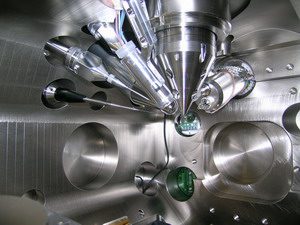
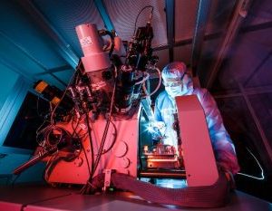
VI. Pictures and misc
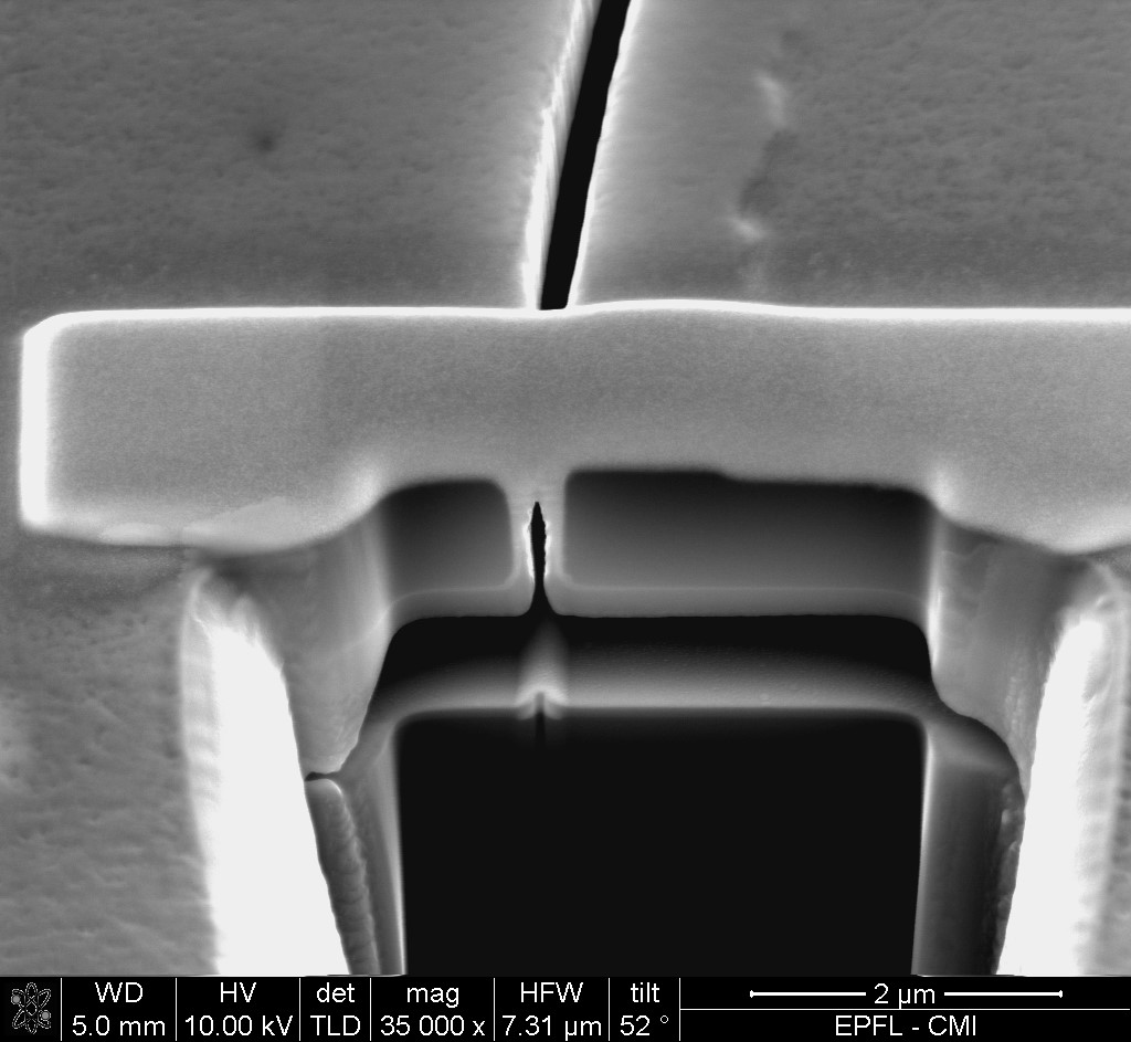
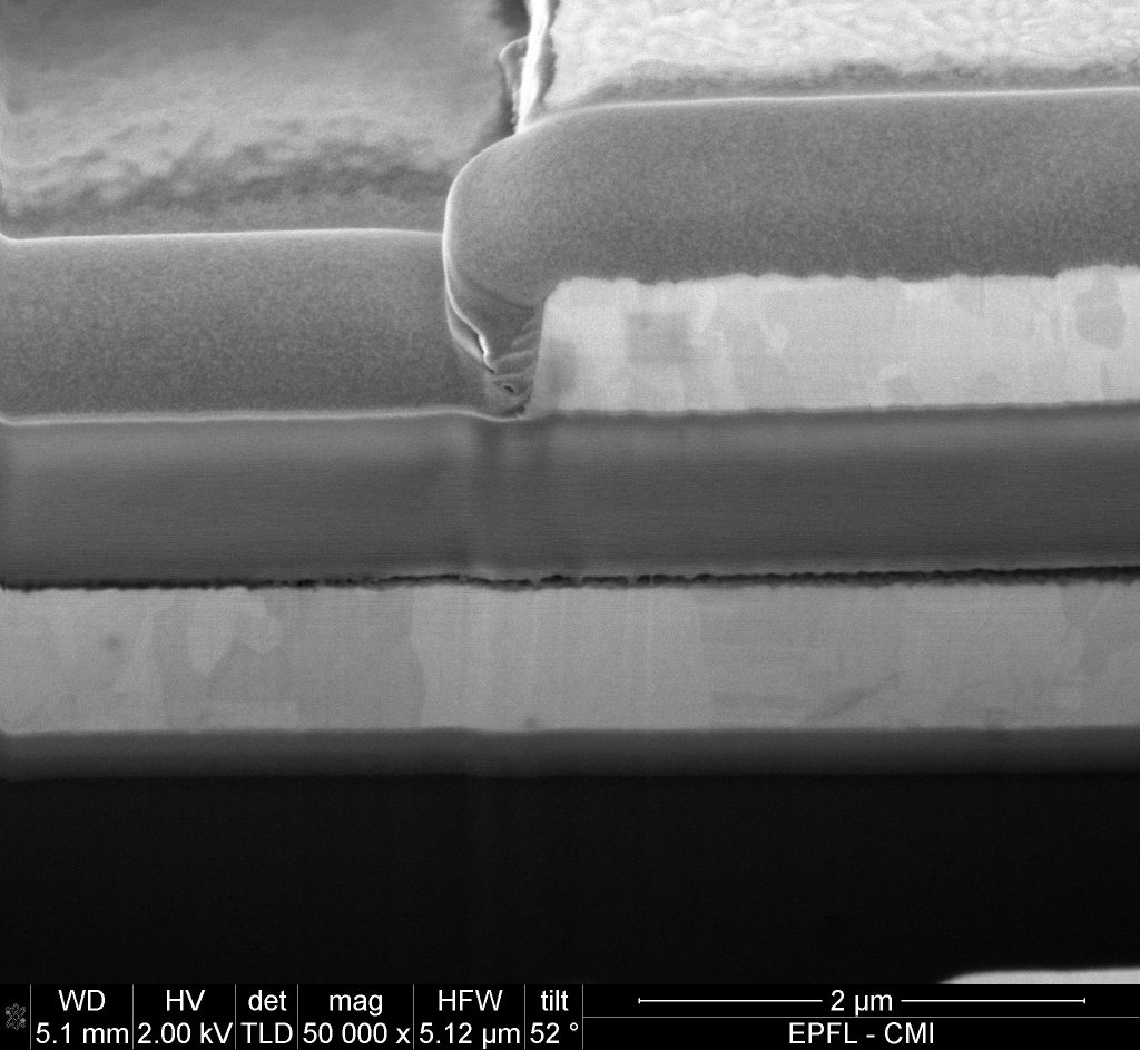

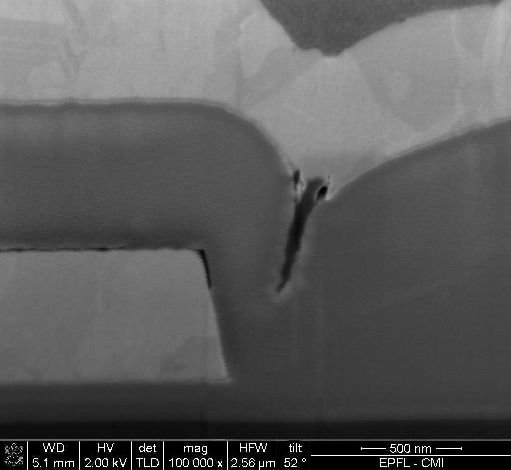
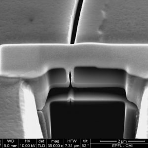

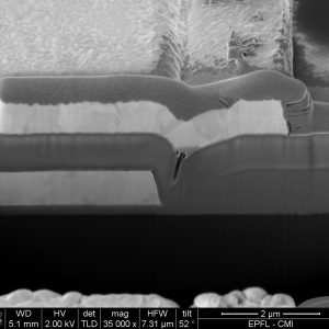
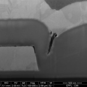
- Below are listed the typical sputtering rates for various materials with ions accelerated at 30 kV. The exact value will depend on patterning conditions such as dwell time, overlap…
Material Sputtering rates
([µm]3[nC]-1)C 0.18 Si 0.27 Al 0.3 Ti 0.37 Cr 0.1 Fe 0.29 Ni 0.14 Cu 0.25 Mo 0.12 Ta 0.32 W 0.12 Au 1.5 MgO 0.15 SiO2 0.24 Al2O3 0.08 TiO 0.15 Si3N4 0.2 TiN 0.15 Fe2O3 0.25 GaAs 0.61 Pt 0.23 PMMA 0.4
- In the following table, the time needed to mill a 10 µm x 10 µm x 5 µm box for the previous materials is reported according to the previous sputtering rates. The time is given for two different ion beam currents:
- 100 pA for fine milling
- 5000 pA for coarse milling
Material Time in hours
Fine milling (100 pA)Time in minutes
Coarse milling (5000 pA)C 7.7 9.3 Si 5.1 6.2 Al 4.6 5.6 Ti 3.8 4.5 Cr 13.9 16.7 Fe 4.8 5.7 Ni 9.9 11.9 Cu 5.6 6.7 Mo 11.6 13.9 Ta 4.3 5.2 W 11.6 13.9 Au 0.9 1.1 MgO 9.3 11.1 SiO2 5.8 6.9 Al2O3 17.4 20.8 TiO 9.3 11.1 Si3N4 6.9 8.3 TiN 9.3 11.1 Fe2O3 5.6 6.7 GaAs 2.3 2.7 Pt 6.0 7.2 PMMA 3.5 4.2
Bibliography
-
- Melngailis J. Critical review: focused ion beam technology and applications J. Vac. Sci. Technol. B 5 (1987) 469-495
- Reyntjens S. and Puers R. A review of focused ion beam applications in microsystem technology J. Micromech Microeng. 11 (2001) 287-300