Restrictions and Precautions
1. Maximum allowed booking per person between 9am and 5pm is 2 hours. It is still possible to get 4 consecutive hours from 7am to 11am or from 3pm to 7pm.
2. Reservation names must correspond to operators.
Contents:
I. Introduction
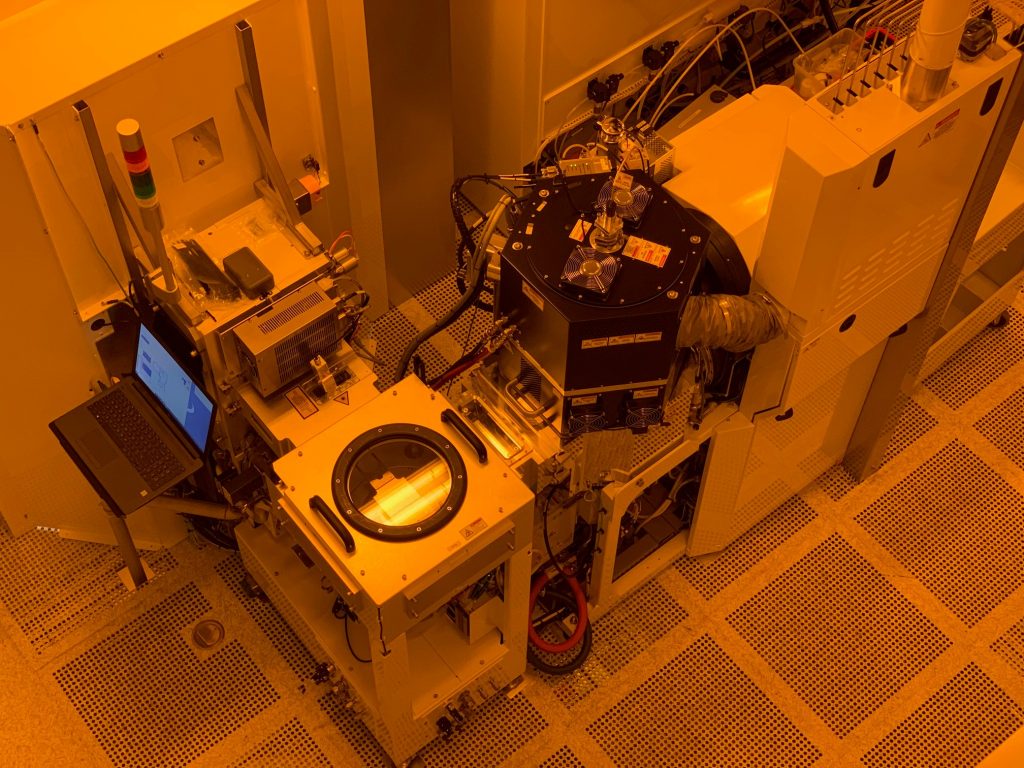
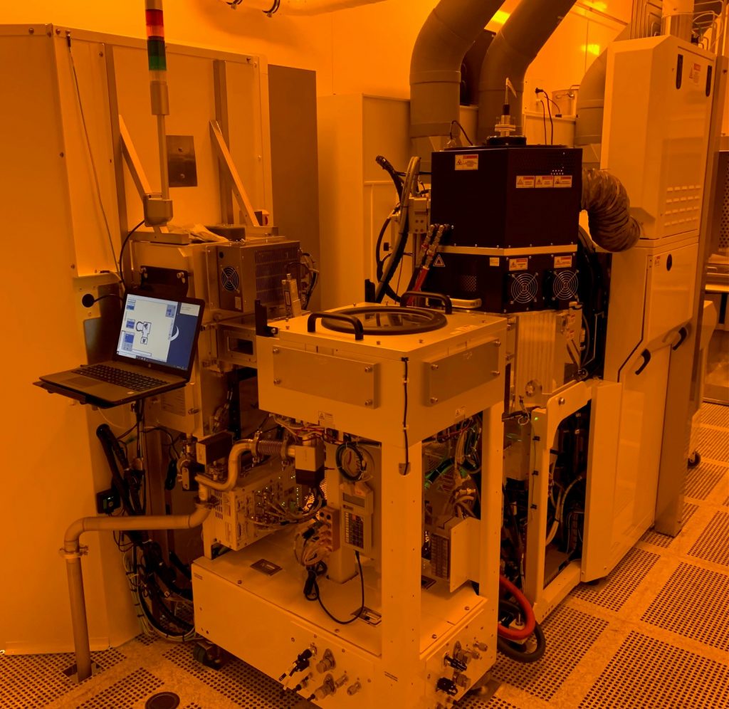
SPTS Rapier etcher is an optimized Deep Reactive Ion Etching (DRIE) system for Silicon (Si) and Silicon on Insulator (SOI) wafers. It includes:
- Single vacuum cassette loader – 25 wafers capacity
- Brooks Magnatran 7 transport robot
- A dual high density Inductive Coupled Plasma (ICP) source
- An Electrostatic Clamping Chuck (ESC)
- Radio and low frequencies wafer biasing, with pulsing possibility
- High speed digital mass flow controllers
- Amplified optical emission spectroscopy end-point-system
- White light interferometry end-point system
- Powerful software with possibility of various ramping curves of all process parameters with time
II. Rapier module
SPTS Rapier module is a unique, patented dual plasma source, that offers high flexibility with multiple operating modes.
SPTS Rapier module is fitted with two RF independent sources (up to 3kW), and two independent gas showers (center and edge zones) for excellent uniformity at improved etch rates control.
The module includes a high-efficiency, thick dielectric, bipolar electro-static clamping (ESC) with variable clamp voltage. Temperature control ranges from -10°C to 30°C.
Wafer biasing is possible as radio frequency (up to 2kW) or low frequency (up to 1.2kW), both with pulsing possibility and control of the duty cycle.
Chamber plasma conditioning or self-cleaning can run as wafer-less if needed.
Available process gases are 2x SF6 720sccm, 2x C4F8 500sccm, O2 300sccm & 1000sccm, Ar 500sccm, N2 100sccm.
III. Standard processes & usermanual
| Process | Average etch rates* | Remarks |
|---|---|---|
| DRIE | Trench 2um: 300nm/loop. Trench >200um: 800nm/loop. | If O2 descum step: initial PR removal of 10nm/sec. Notch on SOI <300nm. PR etch rate 6nm/loop. SiO2 etch rate 2.5nm/loop. |
| High Aspect Ratio (HAR) | Hole 10um: 200nm/loop. Trench 2um: 165nm/loop. | SiO2 hard mask required (etch rate of 2.5nm/loop). Last 300nm of mask not viable because of faceting. |
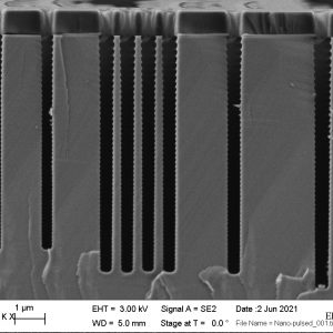
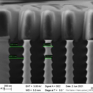
| DRIE-Nano | Trench 350nm: 150nm/loop. | For sub-microns patterns. Scallops <50nm. Depth limited to tens of um. |
| Opto | From 130nm/min to 370nm/min. (several recipes) | Continuous etch process. For shallow and accurate etch. For less than 2um deep. SiO2 etch rate 20nm/min. PR etch rate 40nm/min. |
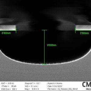
| Si_Release | ~3um/min lateral ~6um/min vertical | Continuous etch process. Isotropic etching of Silicon. |
| Oxide_RIE | SiO2: 235nm/min Si3N4: 110nm/min | PR etch rate 170nm/min. Thin layers only (<1um). O2 cleaning compulsory. |
| BARC | DUV42P: 78nm/min Si: 50nm/min | Anti-reflective coating opening after DUV litho. |
| Wafer thinning | 4.4 um/min. | uniformity +/- 3.5%. |
| Dicing | Design dicing streets only (150um): 3.4um/loop Design 25% Silicon load: Trench 100um: 2um/loop Trench 20um: 1.5um/loop | Very large scallops/mask under etch of ~2um. Trench 200um: negative profile ~2° off vertical. SiO2 etch rate 4nm/loop _ PR etch rate 8nm/loop Not for structures <10um (too large CD loss) |
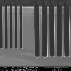
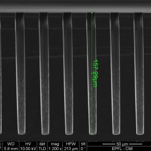
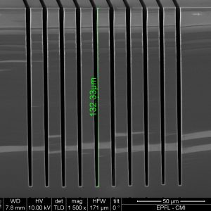
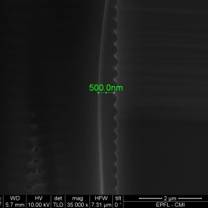
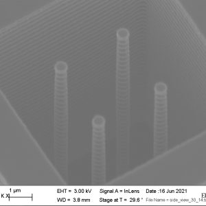
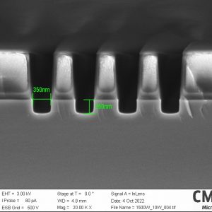
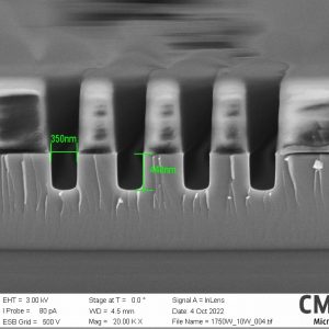
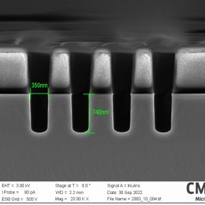
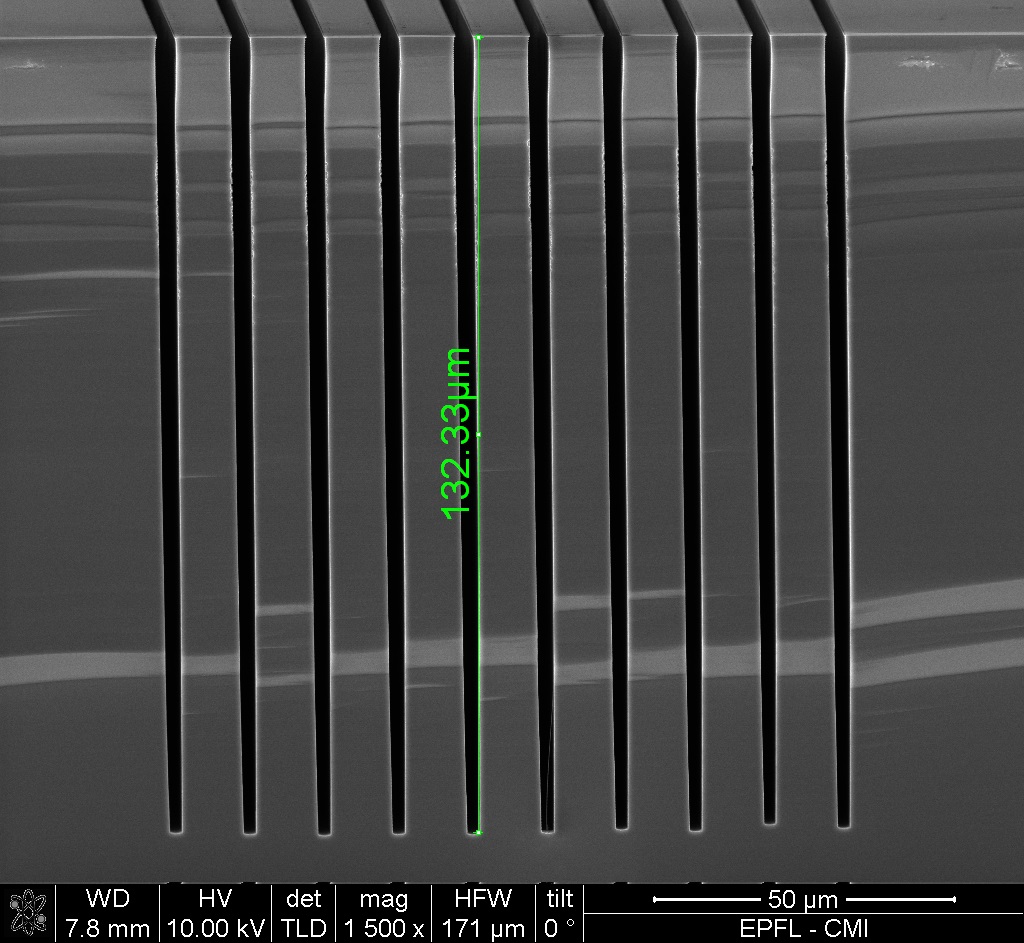
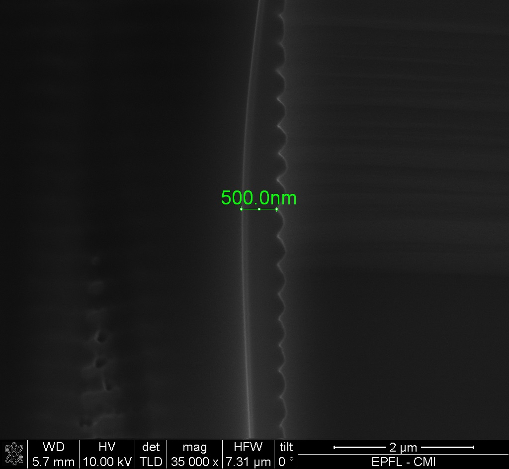
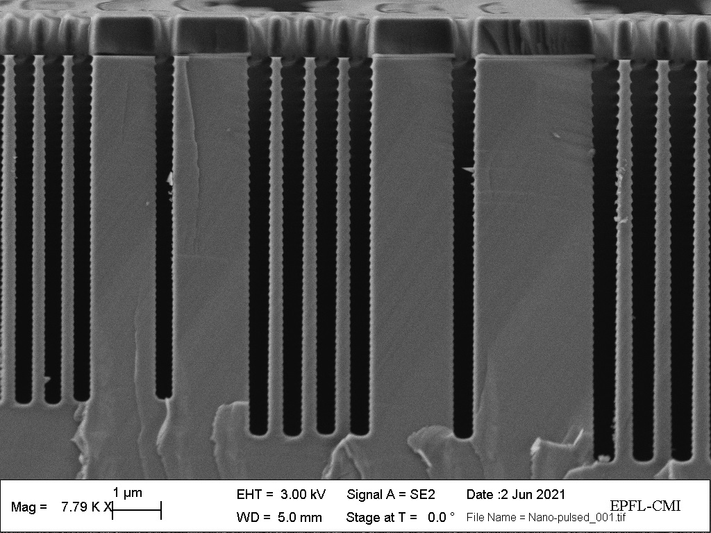
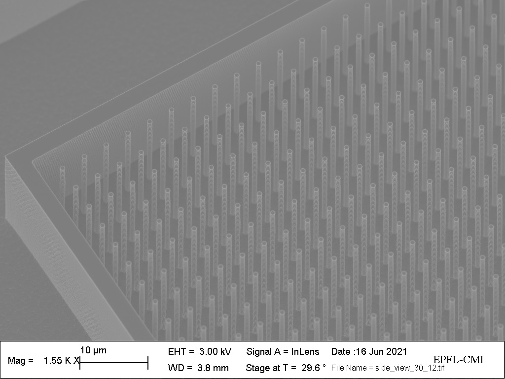
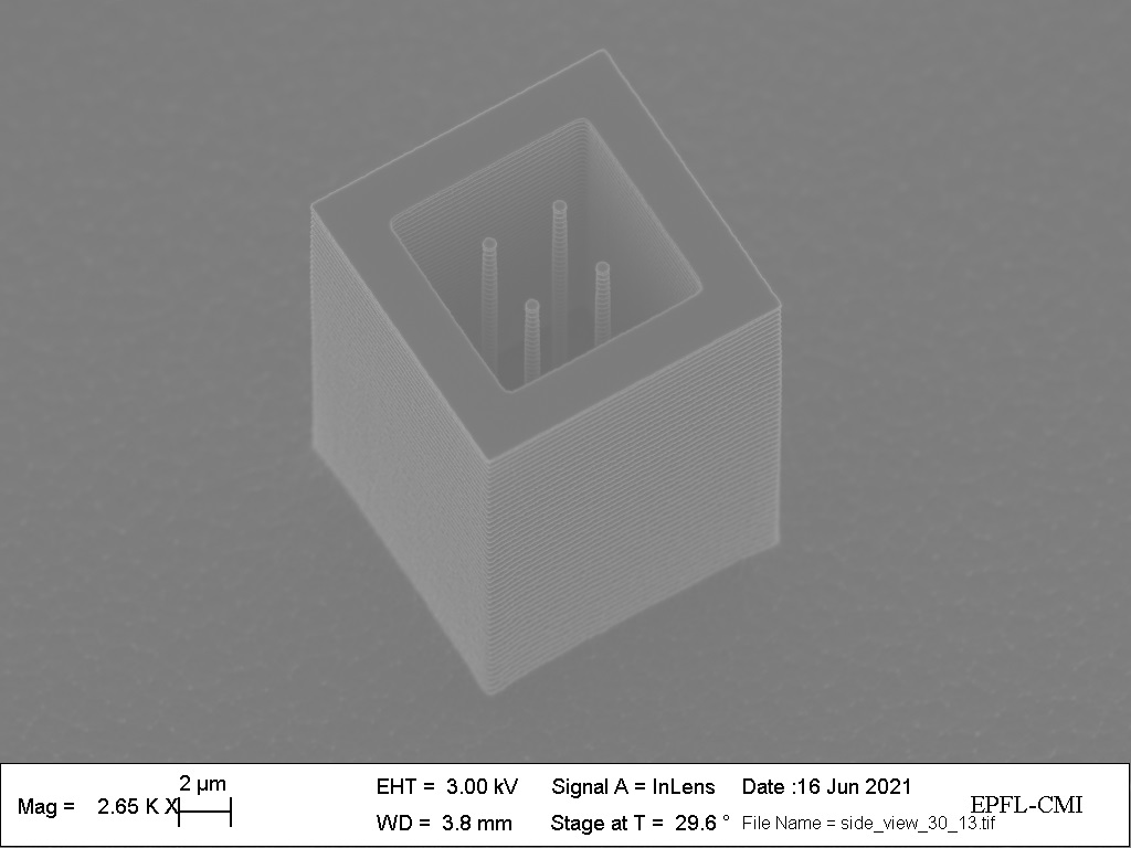
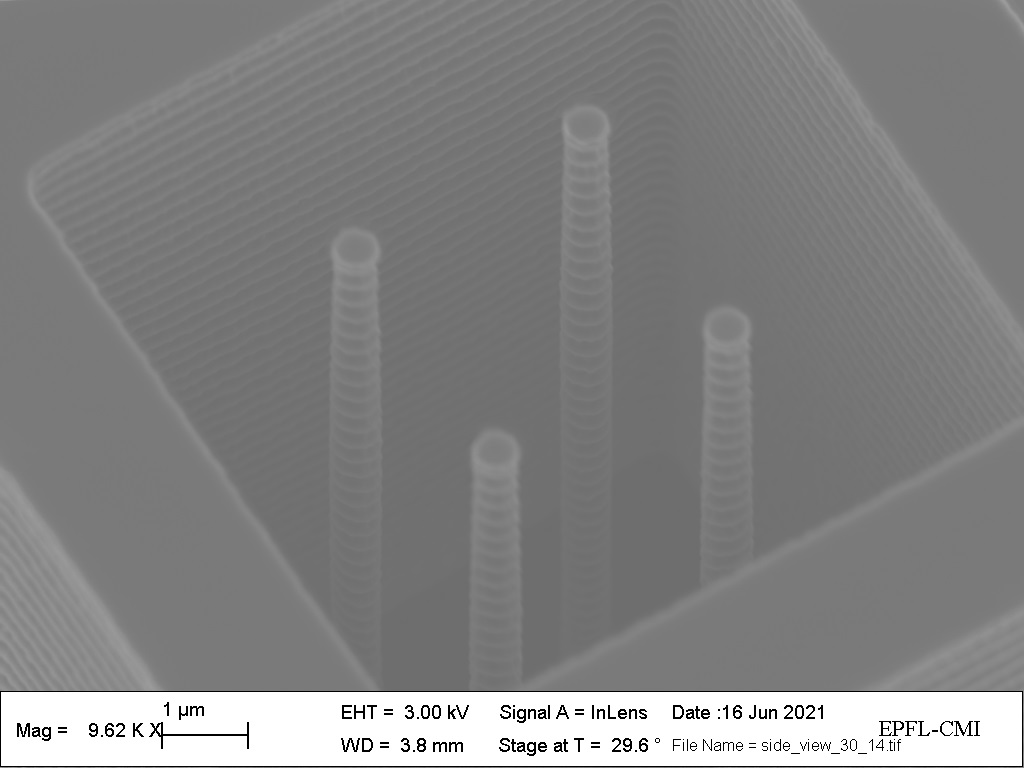
IV. Photo gallery
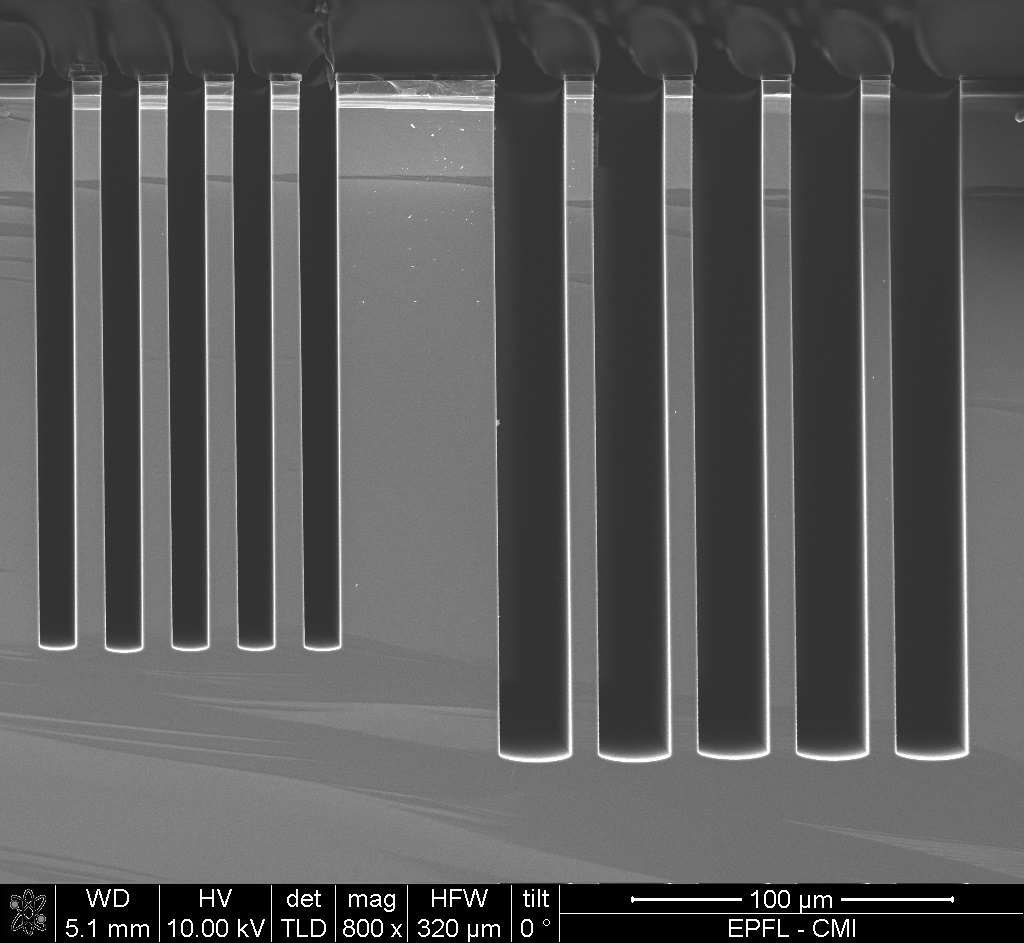
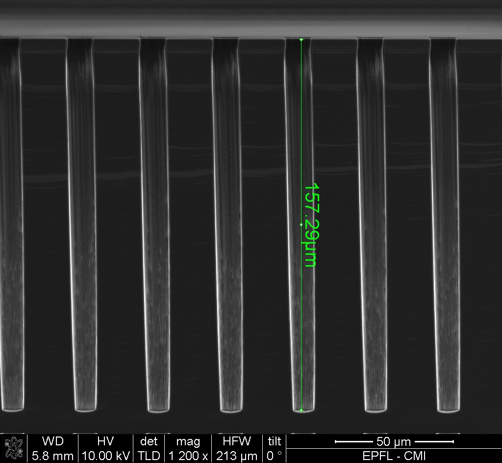
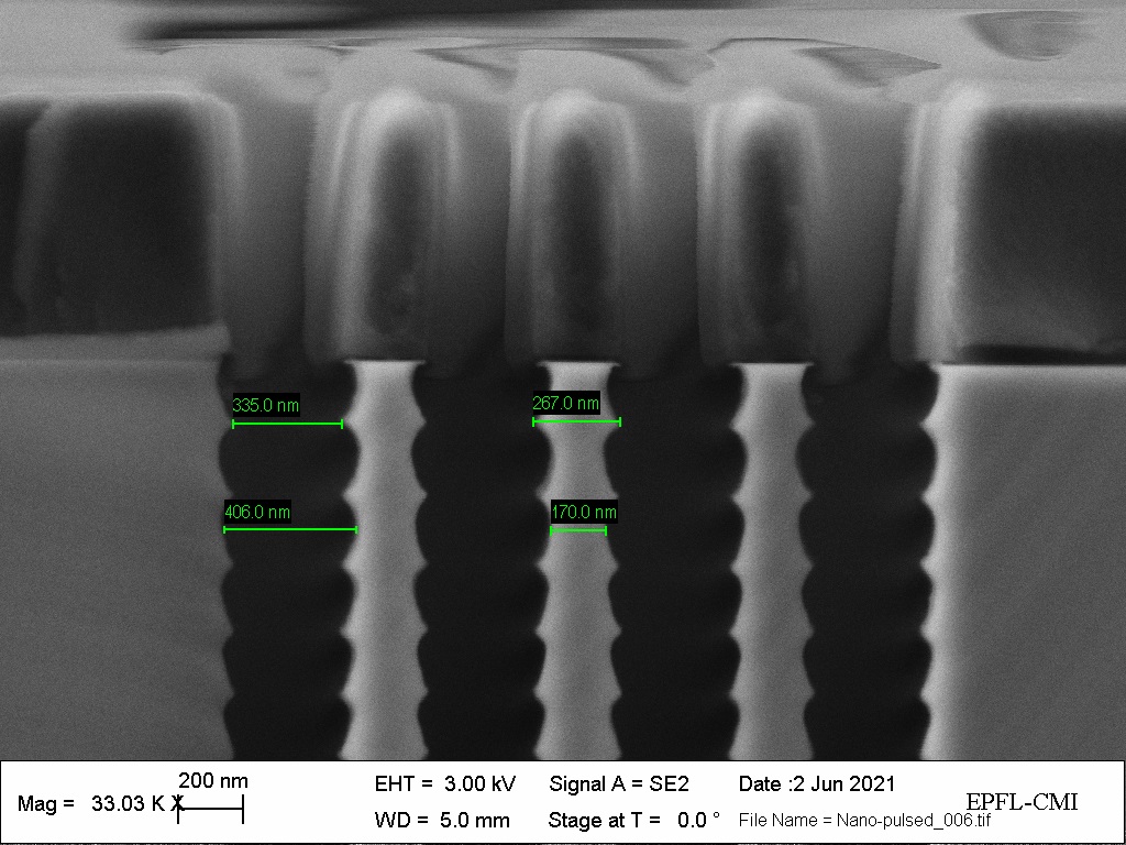
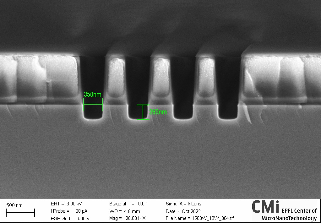
2min etch time
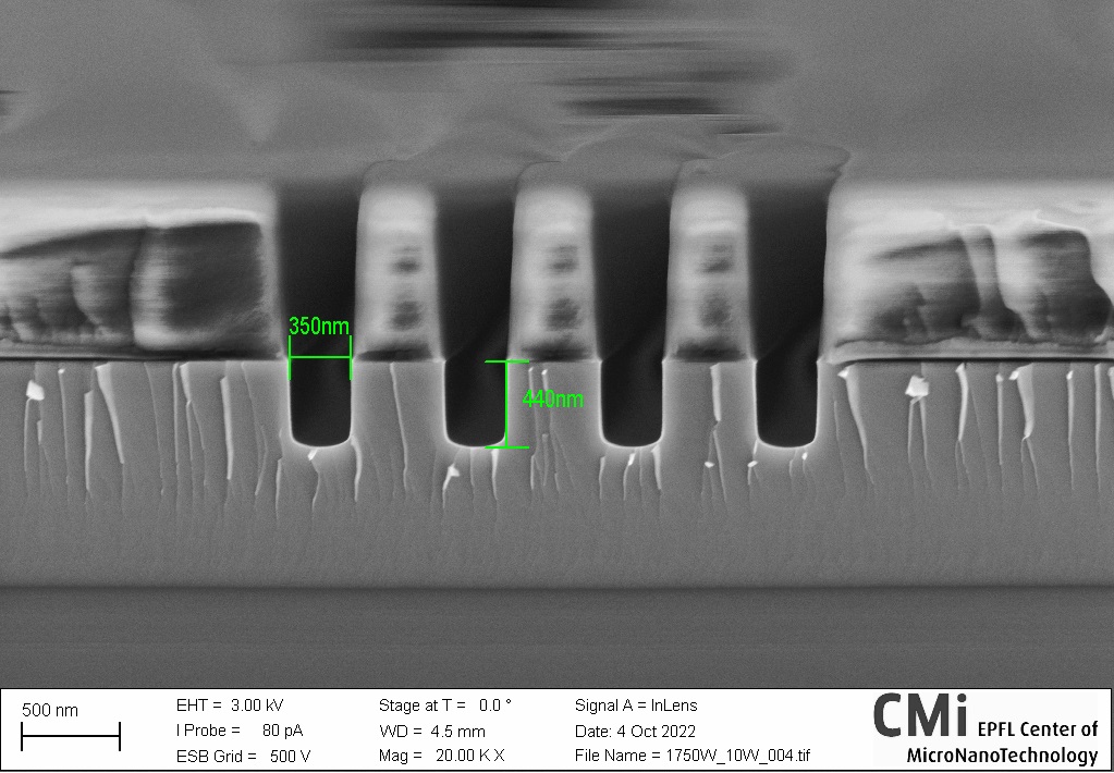
2min etch time
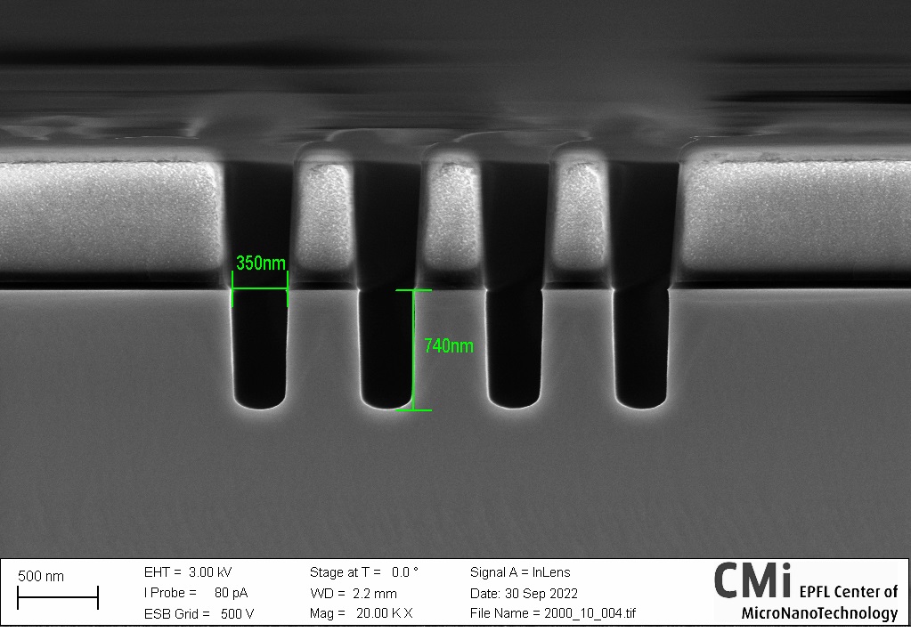
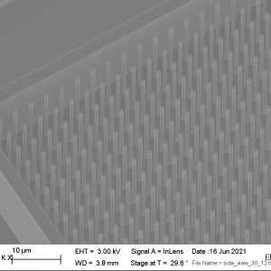
2min etch time
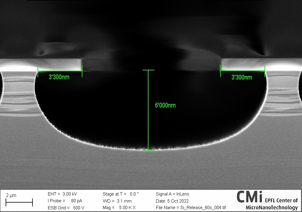
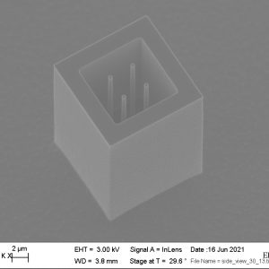
60s etch time