Back to the current year Winners
2022, December
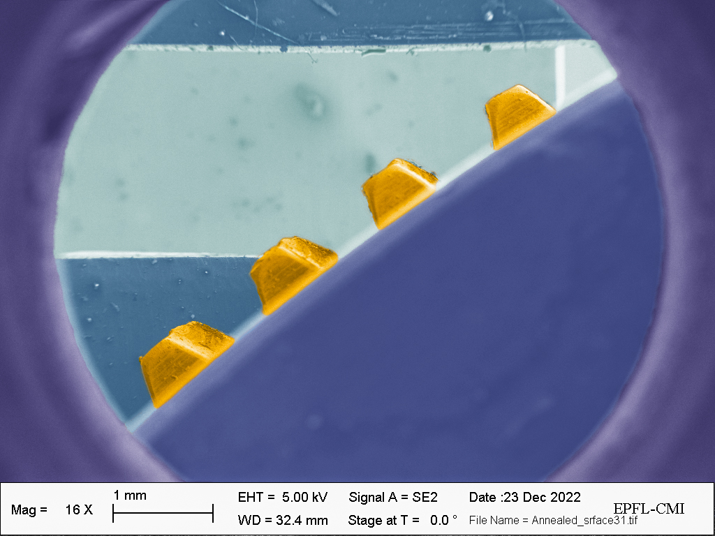
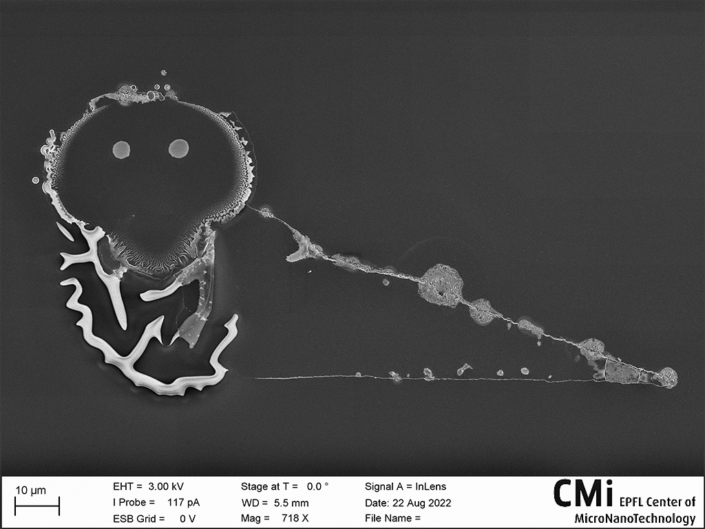
Finally, LEO’s selfie
Daniel Moreno Garcia, NEMS
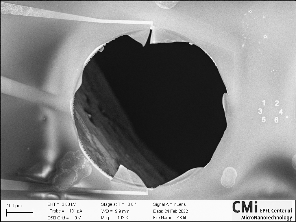
For years, LEO has taken hundreds of thousands of images for us. However, as the beginning of its retirement nears, LEO wanted to enjoy the spotlight for once. With this selfie, LEO shows us, through a holder hole, the gears that allow sample rotation. LEO feels in good shape and until the last day, will continue to happily wobble for us.
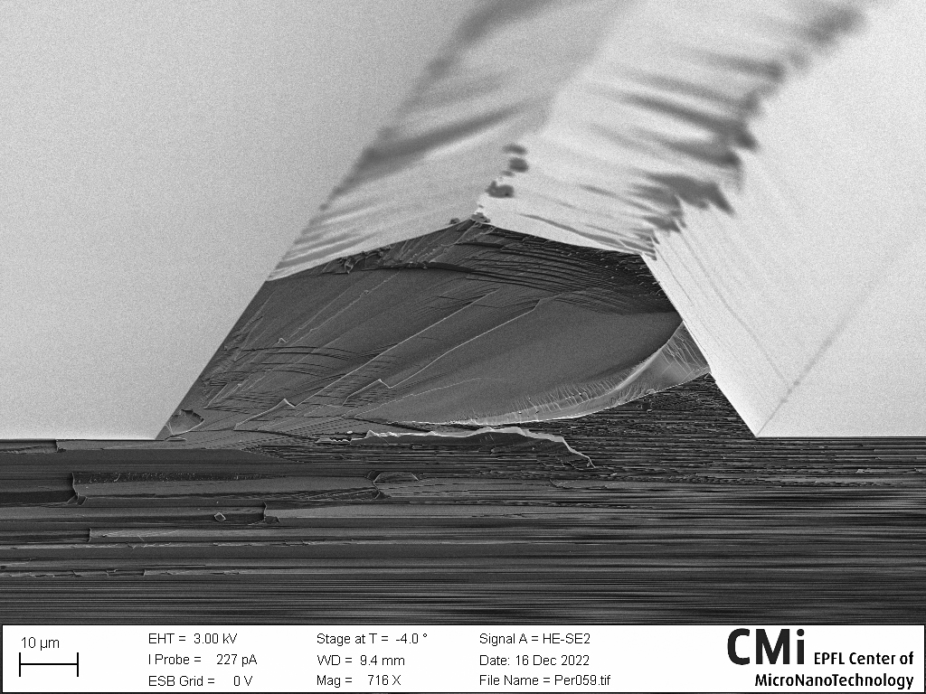
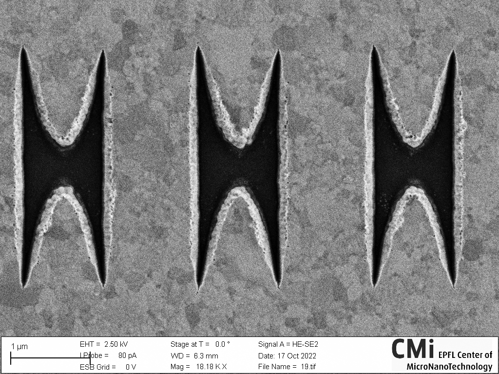
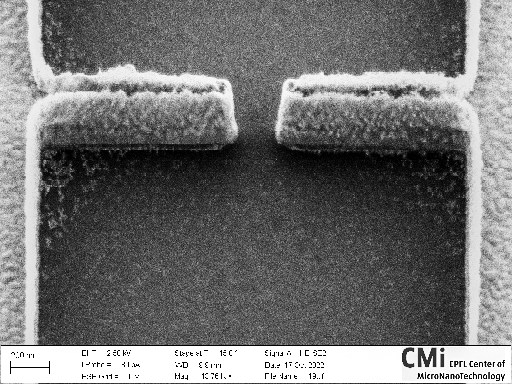
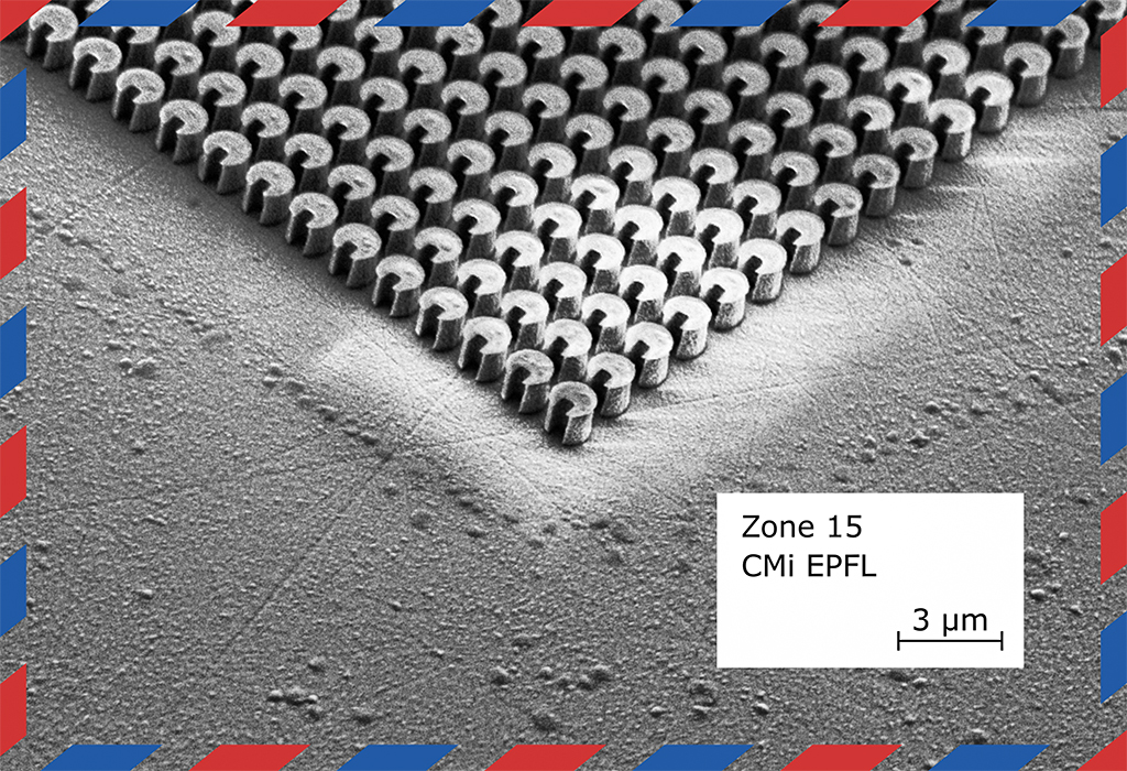
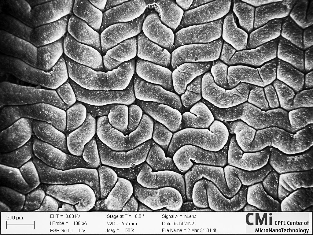
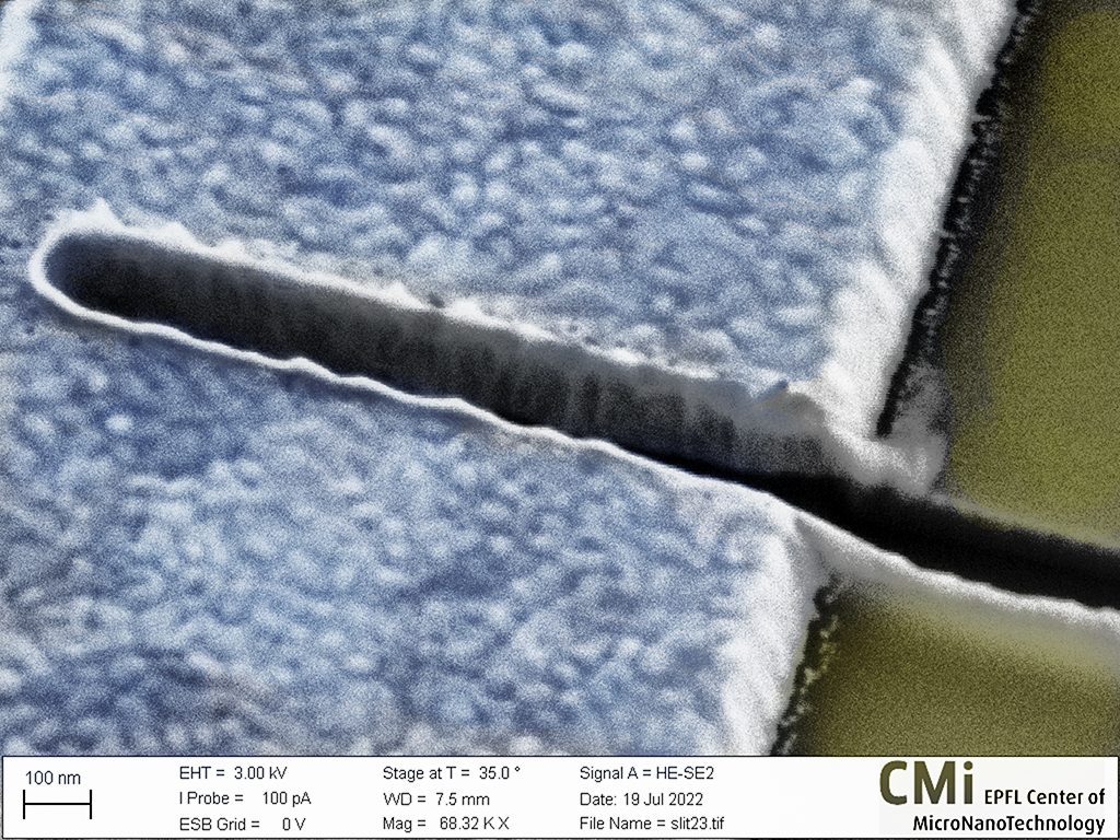
HARDERGRAT
Mohammad Matin Behzadi, LMIS4
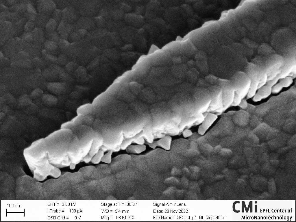
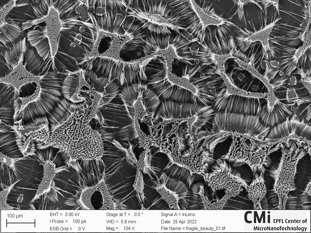
The Hardergrat is known as one of the toughest day-hikes in Switzerland and also one of the most dangerous. The trail begins at Brienz and runs along the Brienzersee (Brienz Lake) all the way to Harder Kulm Station. What you see in the picture is the section of a silicon microblade that has been fabricated by lithography and two steps of wet etching with KOH. This blade is used as a mold in the nanopositioning system to make a nanopore.
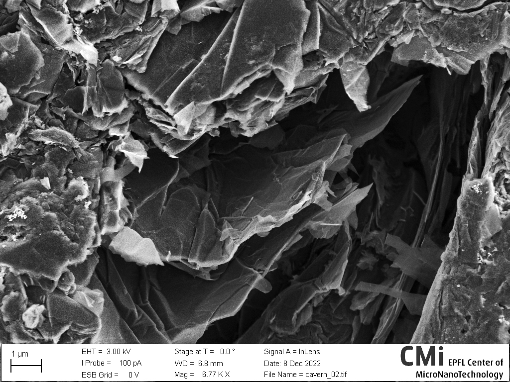
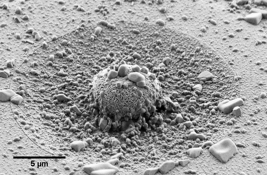
Cavern
Philippine Catherine Marilyn Milward, MT-MA3
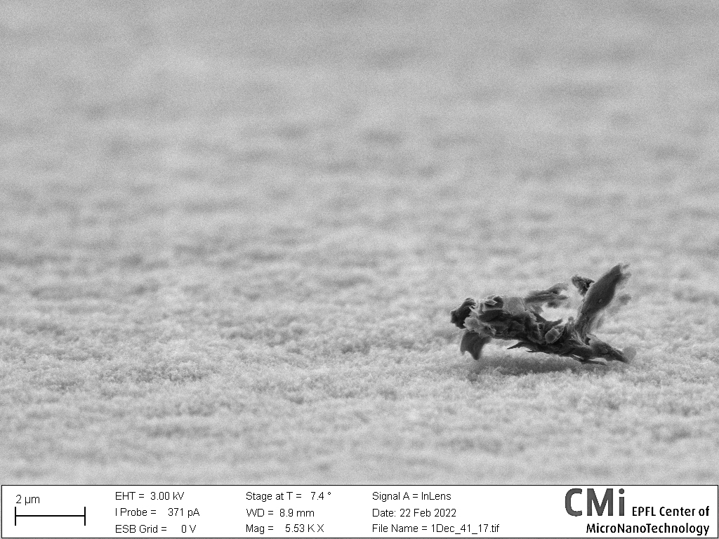
Could a monster be hiding at the end of this cavern? Is this why only a few electrons manage to escape and fly back to the safety of the SEM’s sensors? Only the maddest scientist could imagine what a creature like that could look like.
2022, November
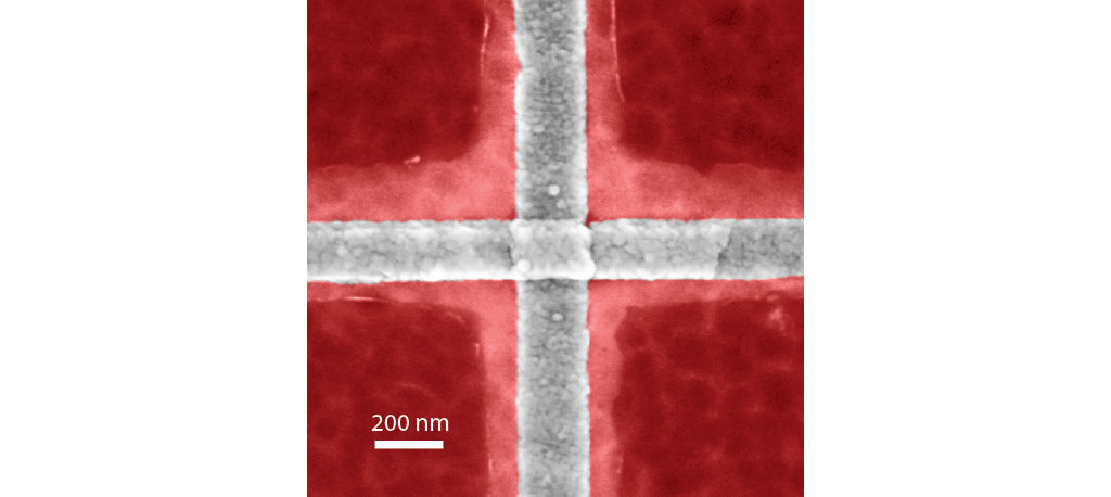
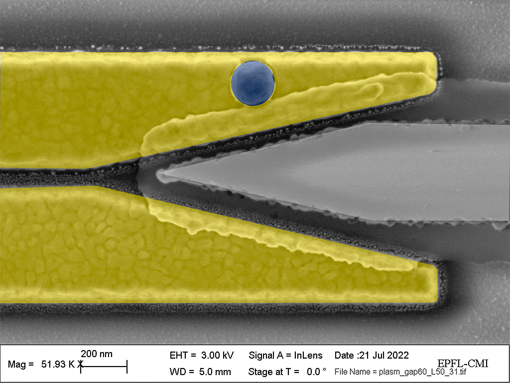
Quantum Swiss Flag
Mahdi Chegnizadeh, LPQM1
Josephson junction is a tri-layer structure of superconductor-insulator-superconductor. The nonlinearity that it provides at microwave frequencies enables us to have artificial two-level systems, quantum bits, which opens the door toward the quantum realm. The junction is , Manhattan style, made in-situ using shadow evaporation technique in an ultra-high vacuum evaporator (PLASSYS) in CMi. When colored properly, it resembles the Swiss flag!
Nano waves
Xia Liu, LMIS1
Sine wave surface at nanoscale.
Aluminum crocodile
Francesco Bertot, HYLAB
It seems the deposition of aluminum on top of a silicon waveguide became the perfect habitat for this micro-crocodile, who is surfing the Al surface to scout for a prey.
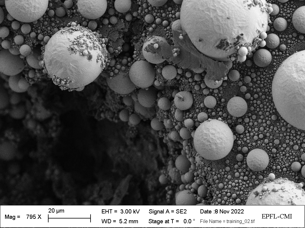
Falling into fractals
Michele Ghini, NANOLAB
Tin microparticles of very different sizes cover everything in the landscape, including themselves.
2022, October
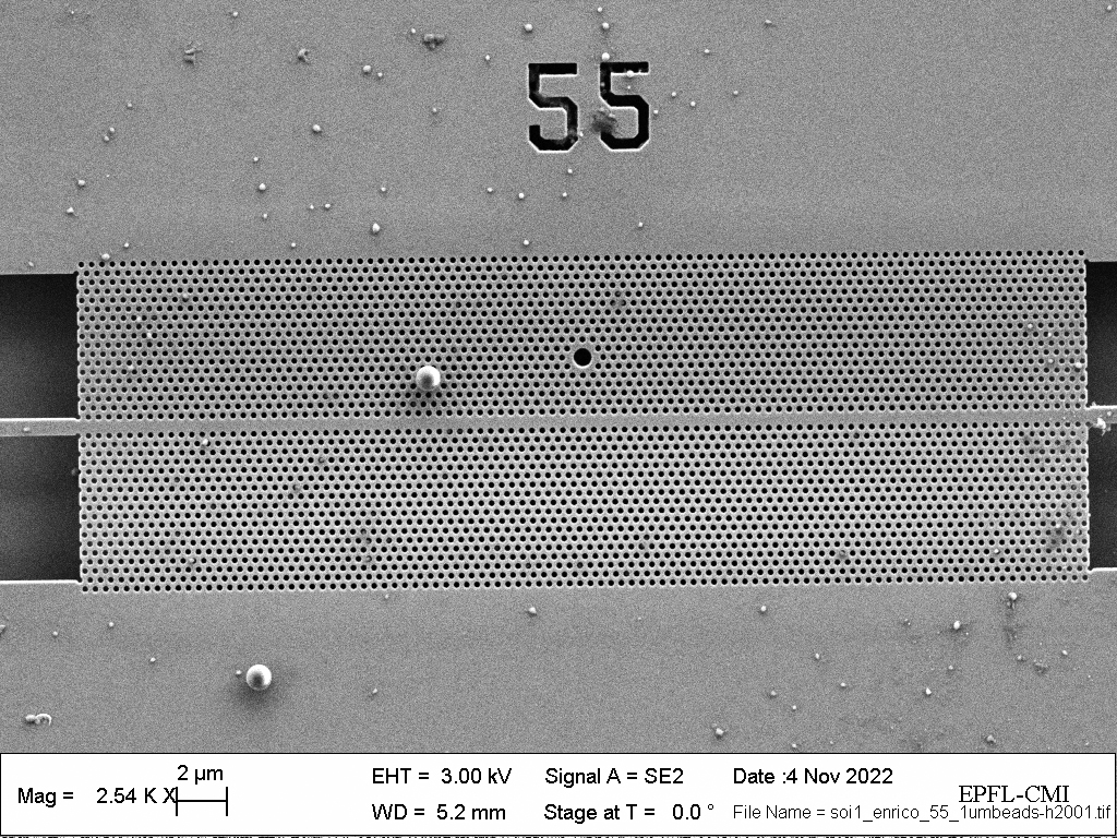
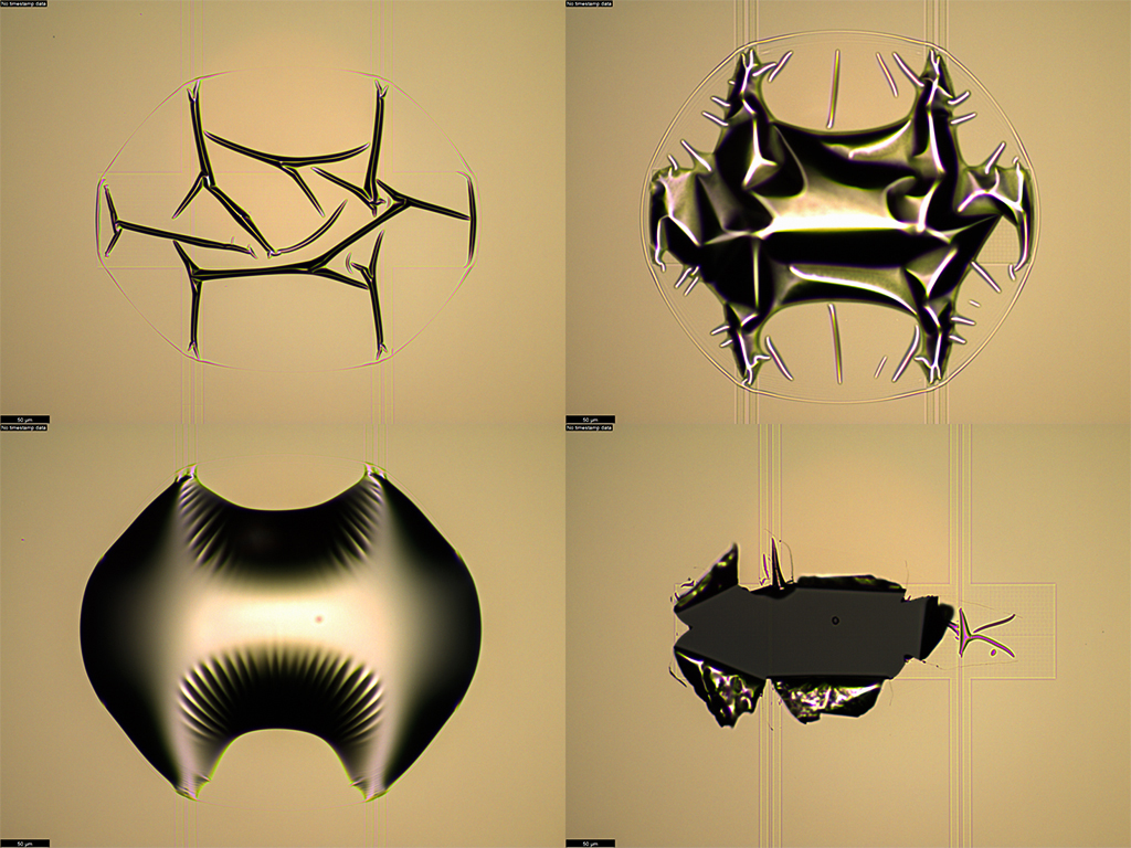
The dead of a polystyrene planet orbiting around a photonic crystal black hole
Enrico Tartari, SCI SB RH
The black hole is a Silicon photonic crystal hollow cavity (750nm diameter) that confines light in such a small volume that an optical trap is formed. Any polystyrene planet (1 um diameter) that, with an excess of arrogance, passes too close to the black hole, will be inexorably trapped.
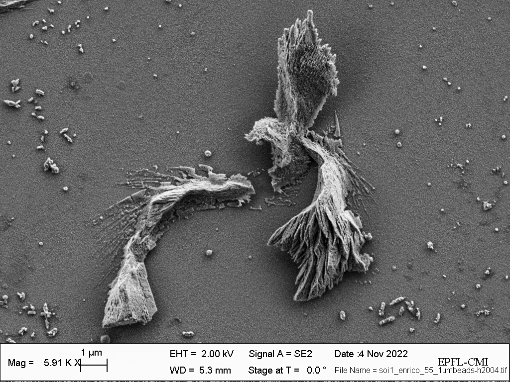
Not harmful is all evil: a contaminant phoenix returns to the nest
Enrico Tartari, SCI SB RH
In a hectic world it is good to know how to stop for a moment and admire the beauties that nature offers. Like a dusty family album, here’s what you can observe by investigating an old disused silicon chip, in which dust and small unidentified contaminants have finally found their space.
Batman
Zhiyuan Xie, LQNO
“Maybe that’s what batman is about. Not winning…but failing, and getting back up. Knowing he’ll fail, fail a thousand times, but still won’t give up.” – Batman. The Bat-Signal is now on the night sky. Dear fellows, no matter how tough your research may be, don’t give up!
Farewell
Zhiyuan Xie, LQNO
I am about to depart from this calm harbour for my next grand trip on the sea.
Contemporary Microscopy Art
Didem Dede, LMSC
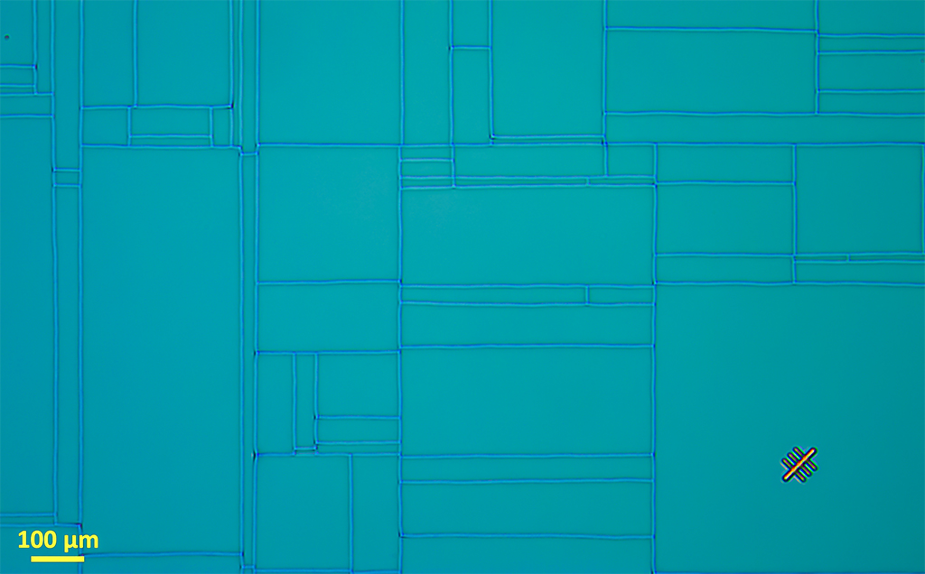
In this latest work of the artist, we see a piece of silicon canvas, painted with ZEP resist, later, soaked into the odorless caustic potash. Brushstrokes at the edges of the wafer reveal the irresistibility between the polymer and the base, leaving some residues at the substrate surface.
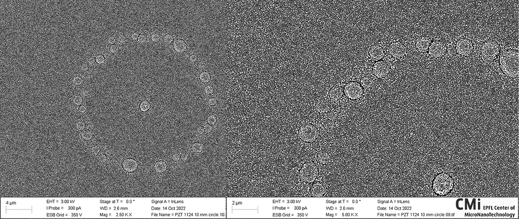
Stonehenge of PZT
Sarunas Bagdzevicius, Piemacs Sarl
Pulsed laser deposition is used not only for state-of-the-art piezoelectric thin film deposition but also for recreation of the historic artefacts. This time it was prehistoric monument from England – Stonehenge. SEM images of the PLD deposited piezoelectric PZT (lead zirconate-titanate) thin film.
2022, September
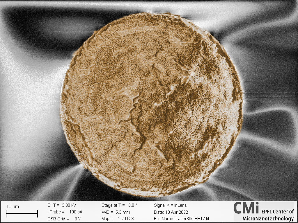
Golden snowfall in a photoresist orchard
Viacheslav Snigirev, LPQM1
Gold lift-off tests with a positive photoresist bilayer on a silicon wafer.
2022, August
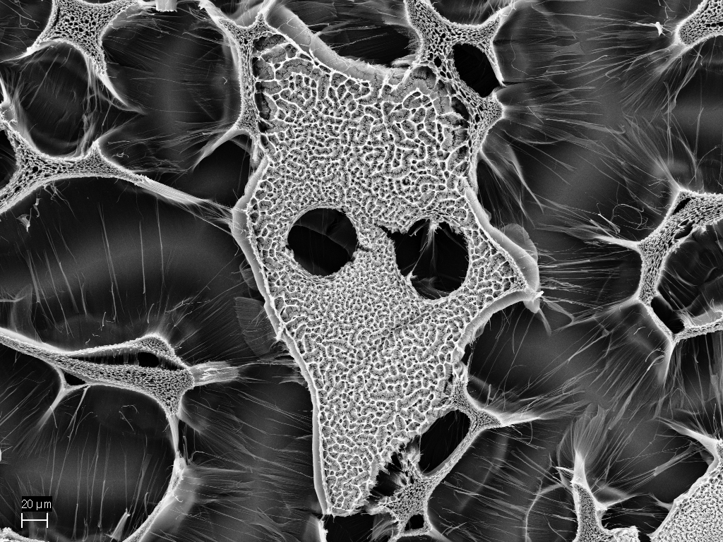
Micro-cemetery
Damien Maillard , NEMS
This micro-cemetery made of silicon nitride stones was build underground by micro-dust and the smallest sorts of contamination to pay their respects. It was uncovered after photoresist was not sufficiently covering the top silicon nitride membrane and could not fully protect it during etching.
Dark side of the moon
Clémentine Lipp, Audrey Jacquillat, LMIS4
This picture of a XeF2 underetching through an opening in alumina makes Pink Floyd melodies run in one’s head and look up to the sky looking for a resemblance.
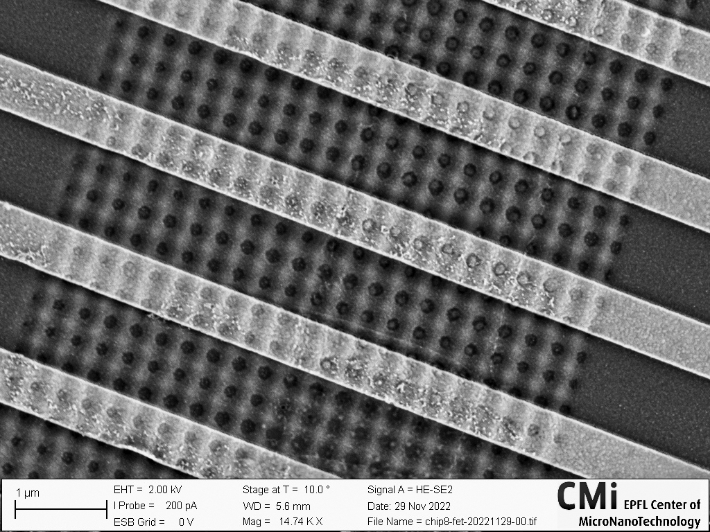
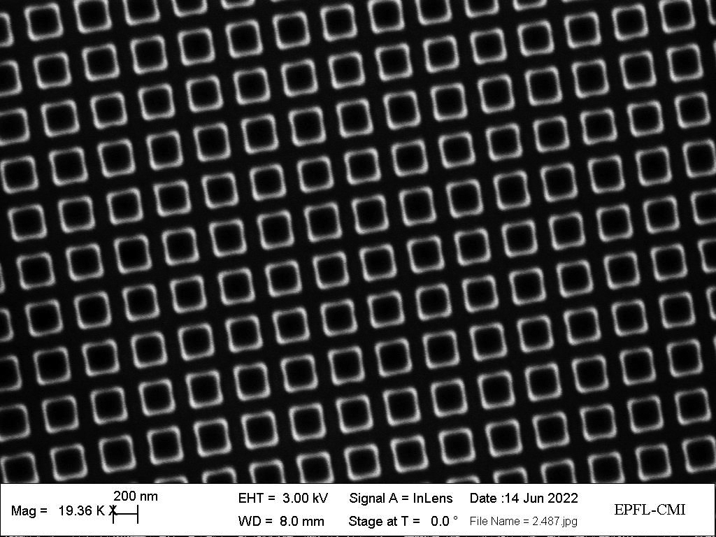
CMi’ve Got Mail
Felix Richter, BIOS
The love letter to CMi shows the square arrangement of mid infrared resonators which at 45° stage tilt reminds of the old days mails. The resonators are etched from amo(u)rphous silicon with an alumina mask.
Overnight invasion
Clémentine Lipp, Audrey Jacquillat, LMIS4
UFO were spotted during the night and are suspected to gather to prepare an invasion. Whether you see avocados or fried eggs on a dark sky full of stars, we are in trouble.
Draught-on-Silicon
Furkan Ayhan, NEMS
The severe drought affecting many regions of Europe since the beginning of the year has been further expanding and found its way into CMi. This is what happens when you evaporate thick chromium on a resist and don’t irrigate it.
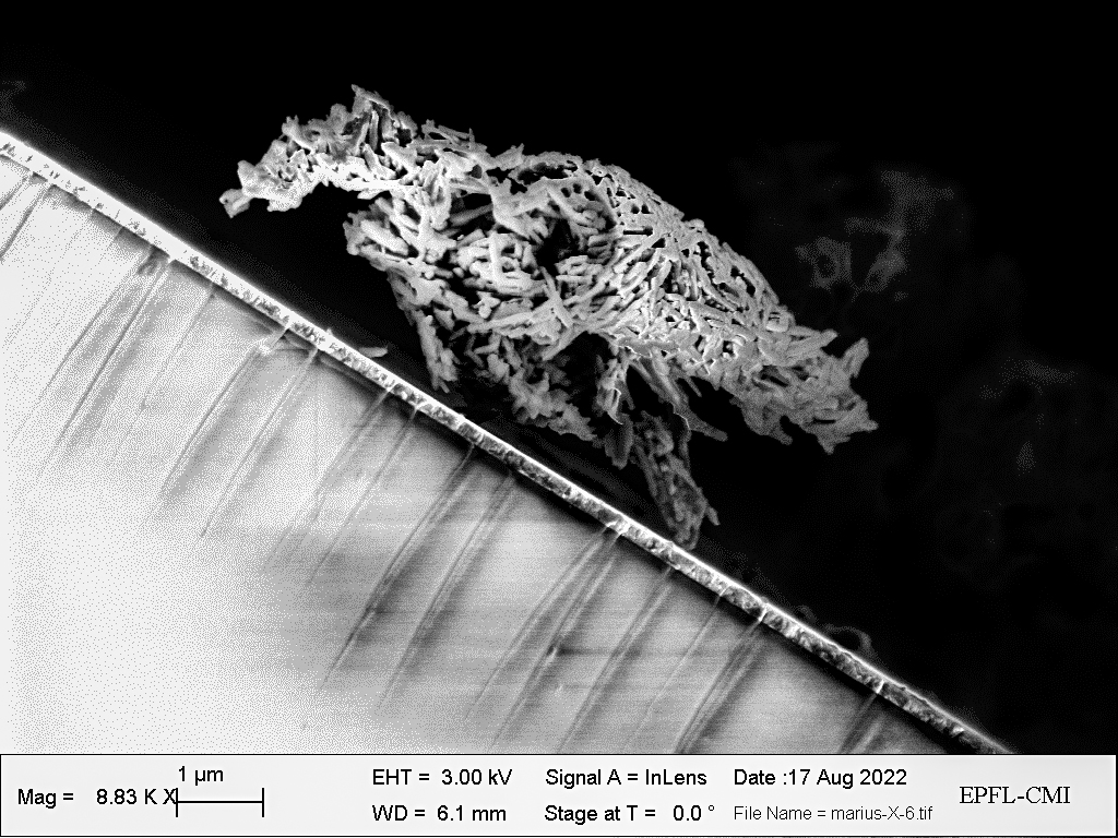
Tiny critter from self-assembly nanowires
Tonglai Chen, Freshape
Not only geckos have the capability to crawl on smooth glass surface. In the nano-scale world, so can our self-assembling nanowire tiny critters.
Fantastic beasts of CMi and where to find them
Giovanni Resta, Unige
The answer is easy: they are already on your wafers !! This very peculiar beast, looking a lot like a tiny walrus (or a young Jabba the Hutt), is made of superconducting NbTiN (sputtered at CMi) and SiO2, and was found on the wafer in a region where e-beam resist had not been properly spin-coated due to a residue. During subsequent SF6 reactive ion etching, nonuniformities in the resist thickness resulted in the birth of this tiny walrus.
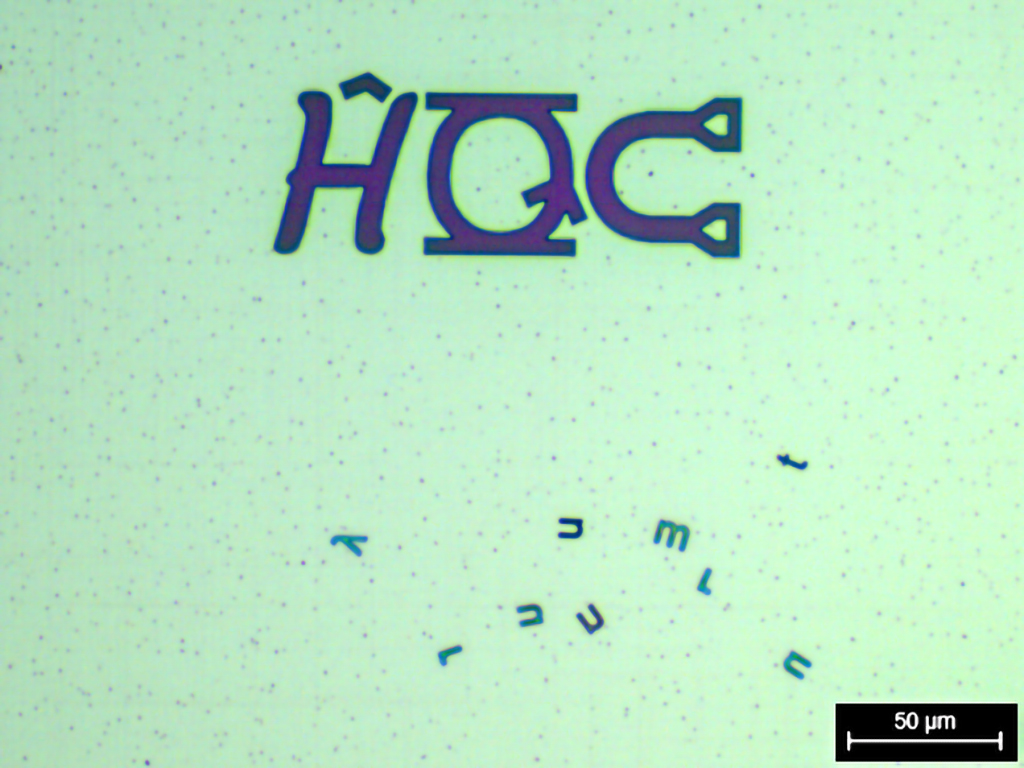
Quantum Soup
Franco De Palma, Nanolab
Who said that quantum mechanics can be observed only at cryogenic temperatures? This picture is the proof that this is not true! In fact, the e-beam lithography tool decided by itself to honor the research on quantum phenomena carried out in our laboratory by randomly throwing the letters composing our logo in a superposition state. Nevertheless, few letters did not survive to this state initialization, so the method has still to be improved in the near future in order to efficiently implement a random letters mixer.
2022, July
Zopft
Victoria Manzi Orezzoli, Nanolab
Vertically aligned carbon nanotubes structures expanded after critical point drying creating braided patterns as in a traditional Zopft.
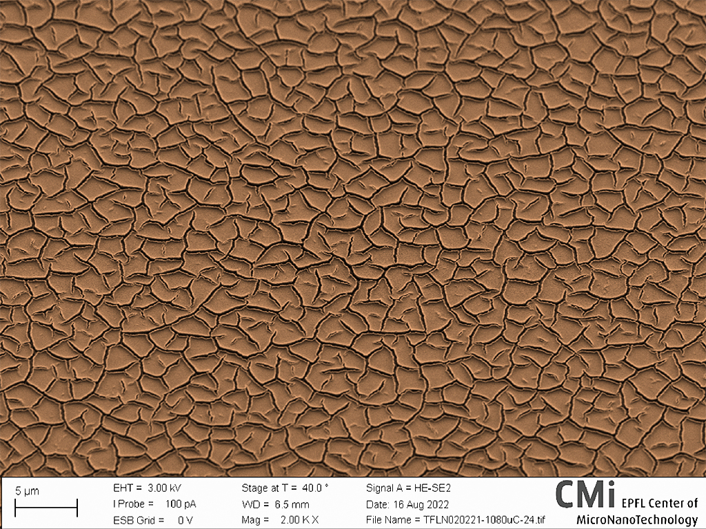
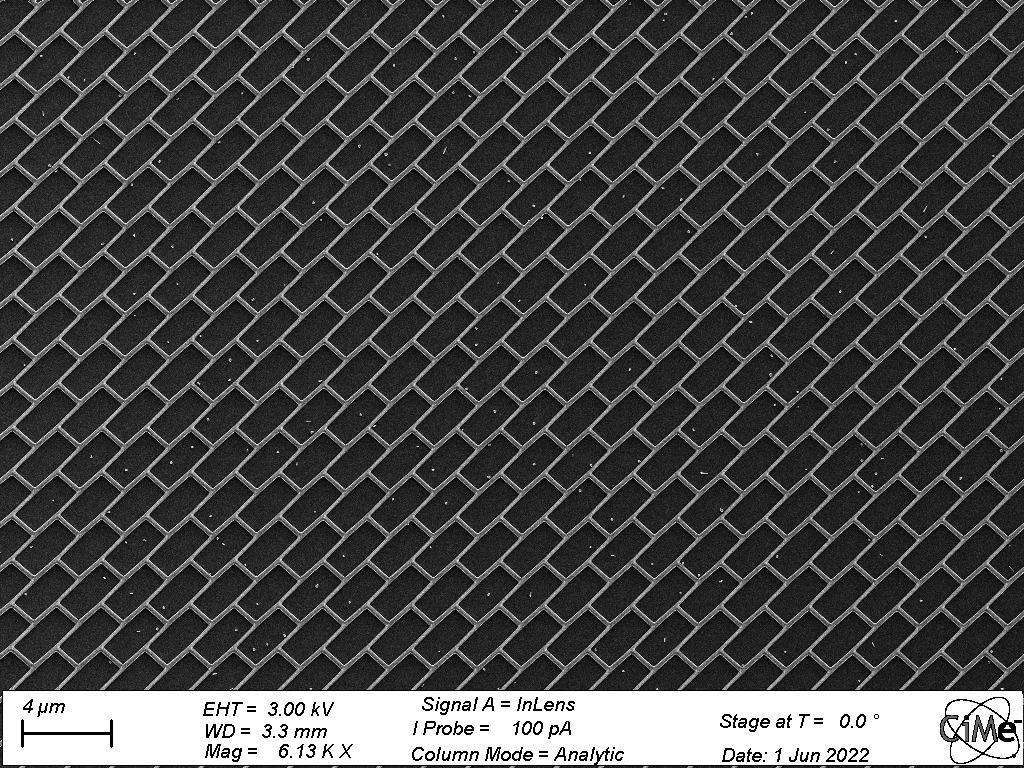
Sardine cannery
Xinru Ji, LPQM1
The stress release patterns for thick silicon nitride films look like sardine cans after etching.
Evil microbrain
Nicolas Maïno, LMIS4
What is this microbrain doing? Same as every night silly, trying to take over the clean room. For now this evil platinum brain is raising an army of salt flakes. Watch out!
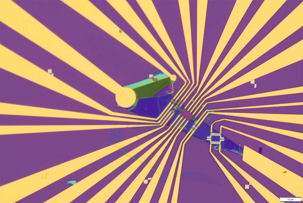
A golden snake is eating the circuit!
Francesco Bertot, HYLAB
After all the time I spent on the process flow, a golden snake started eating all my waveguides! This false-colored structure was obtained after Silicon etching and two consecutive steps of gold deposition, with a gold particle casually forming the “eye” of the snake. Each pattern has been defined through E-beam lithography, obtaining a final gap of only 70 nm.
The bright and dark side of cleanroom
Francesco Bertot, HYLAB
The structure perfectly represents the concept of Yin and Yang: the bright and nice side is actually a bad outcome of an etching step, and will surely lead to a failure in the device. The grey layer of aluminium, indeed, should have been removed before depositing the golden pad. All the features have been patterned through E-beam lithography.
The Lives of Others
Nergiz Sahin Solmaz,
Roberto Russo, LMIS1
Secret service agent is watching the windows of a building in the night.
Parting of the Red sea
Zhiyuan Xie , LQNO
“Then Moses stretched out his hand over the sea, and the Lord drove the sea back by a strong east wind all night and made the sea dry land, and the waters were divided.” (Bible: The Exodus) So it is not only a story! We are the witnesses of the ‘parting of the Red sea’ through the eye of Merlin. On the evaporated ‘sea’ of Gold, a ‘path’ was formed after ion beam etching. Just this time, not a miracle from god, but technology.
2022, June
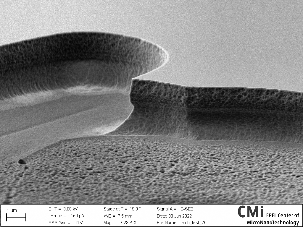
Tiny Grand Canyon
Fabian Oppliger, HQC
This vast 2.5um deep canyon has been formed by erosion due to exposure to an SF6/O2 plasma. The weaker layers of SiGe and Ge on top of a strong base of Si lead to this unique shape of the canyon walls.
Rolex learning center
Hung-Wei Li, Nanolab
During the optimization of the sputtering deposition process, one of the parameters created a non-uniform layer. After observation in the SEM, we found the Rolex learning center in microscale!
Brick wall texture
Hung-Wei Li, Nanolab
After the metal, buffer layer, and catalyst were deposited in CMi, a dense carbon nanotube forest developed on the substrate in a CVD system. We wanted to observe the surface before taking measurements, and we discovered the brick wall texture generated by the carbon nanotube forest!
YAYOI KUSAMA
Chufan Zhou, AQUA
“YAYOI KUSAMA” style nano structure
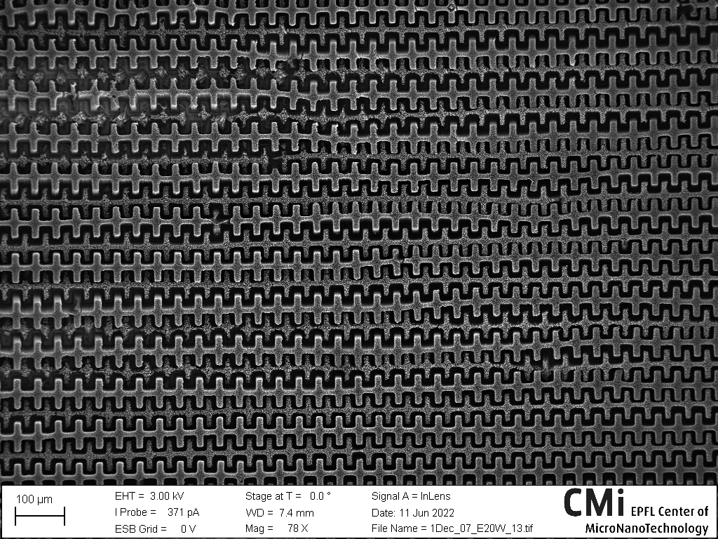
A Nano Brick in the Wall
Valerio Piazza , LMSC
Horizontal 1D III-V semiconductors are promising building block to integrate nanomaterials into existing industrial production flows. The use of a selective mask and epitaxial crystal growth on semiconductor wafer enables the fabrication of nanometric GaAs networks with lithographically designed patterns. One step further toward the goal, Another Brick in the Wall.
2022, May
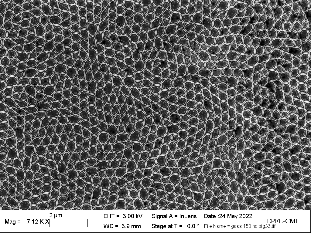
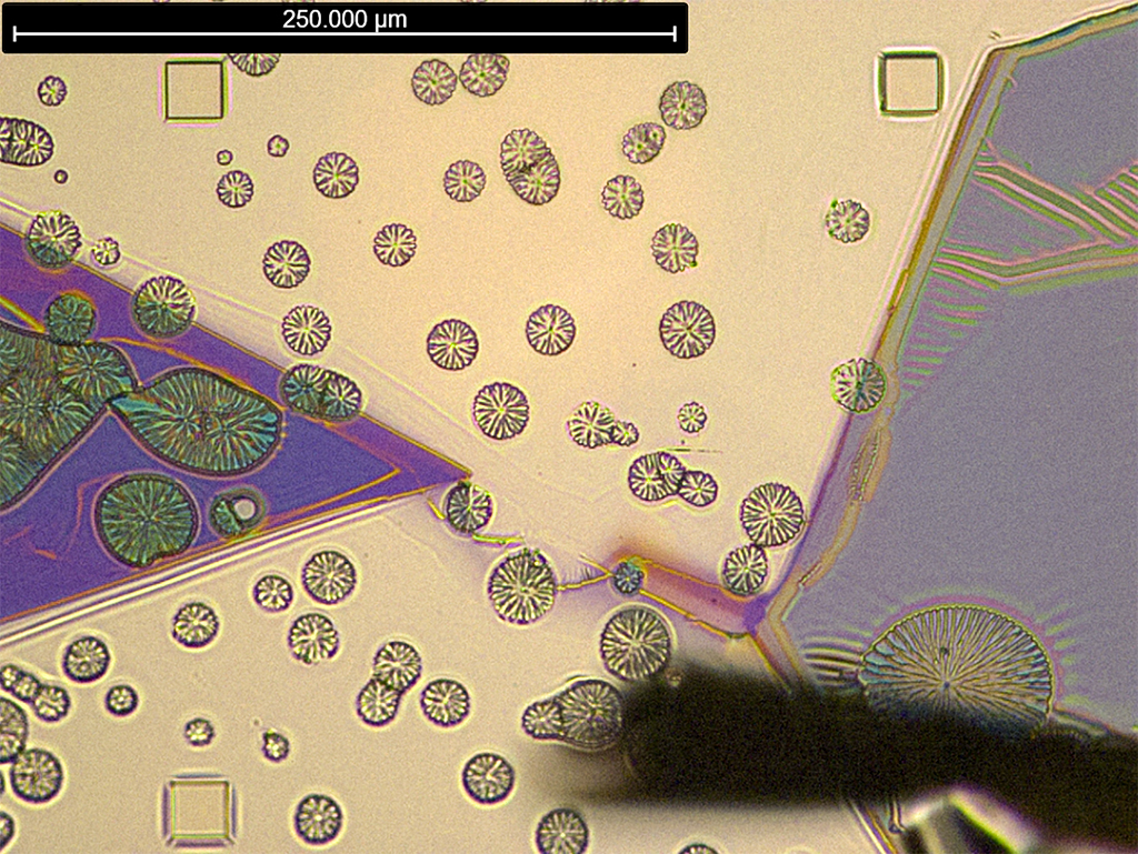
Hyperuniform disorder
Marine Richard, Anja Tiede, LMSC
Does this illusion give you headache? Are you (maybe subconsciously) trying to find an order for these structures? Well, here you see an SEM image of a hyperuniform disordered pattern designed as a honeycomb network that was etched into SiO2 mask on GaAs substrate. In hyperuniform disordered structures there is a hidden order appearing at large length scales. This novel state of matter gains interest because it influences e.g. the photonic properties of the samples rendering them interesting for solar cell or photodetector applications.
Mists in Wadi Rum
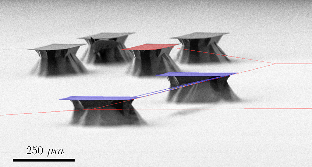
Mohammad Bereyhi, LPQM
Came to life very recently, a mind-boggling creature in CMi, resembling the majestic Wadi Rum: a one-millimeter giant made of high stress silicon nitride, composed of two devices aligned within 100nm distance with the mystical electron beam lithography, suspended with the mysterious chemistry of KOH, and dried by the ineffable magic of critical point drying. This is an optomechanical transducer that bridges the realms of low dissipation MEMS (in red) with high confinement optical structures (in blue) on a single chip. Processes used: EBL, Dry etching, Wet etching, CPD and SEM imaging.
Graphene-nanoelectronics is coming
Artemii Efimov, LQP
The device is a vdW heterostructure based on monolayer graphene that confined between insulating layers of h-BN. The blue-violet triangle is a graphite working as a bottom electrode. Here you can see a classical Hall-bar combining with sputtered superconducting NbTi. Josephson junctions and SQUID from NbTi and Aluminum are seen as well.
Silicon meringue
Nicolas Humblot, Xsensio
Ingredients : 1 silicon wafer, creamy photoresist, oxide flakes, Instruments : etchers, Preparation : a few hours/days in cleanroom.
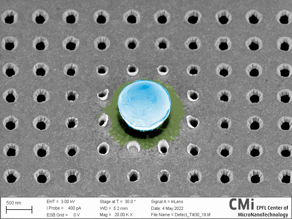
Dome stadium in the nanohole city
Yen-Cheng Liu, BIOS
A dome-shaped metal particle appears in the crowd of plasmonic gold nanoholes. A large clump of metal landed on the patterned structures and it survived the nanohole etching, making it look like a stadium where the show by electromagnetic waves is put on.
Colosseum
Audrey Jacquillat, LMIS4
Two cypress trees in a deserted field overlooked by the Colosseum, this is probably what ancient Rome must have looked like in 70 AD. This historical landscape is actually a tiny set built by focused electron beam induced deposition.
2022, April
Mort
Victoria Manzi Orezzoli, NANOLAB
Post-mortem analysis of vertically aligned carbon nanotubes takes a more literal meaning when a skull shows up in your sample.
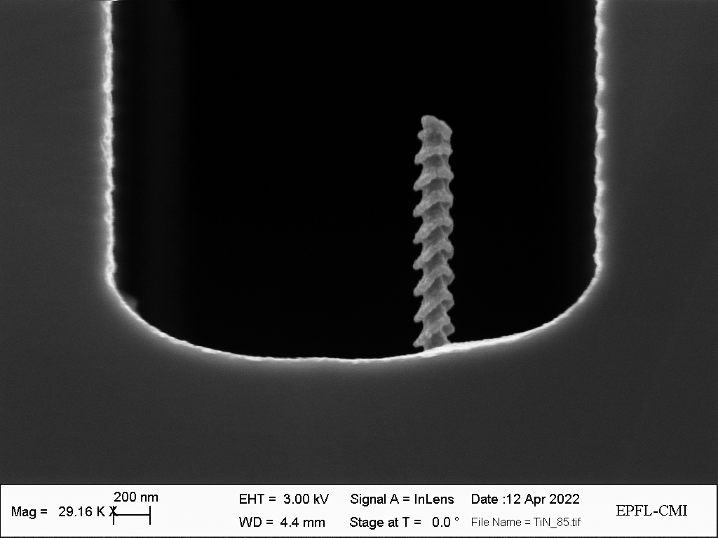
Pisa Tower at CMI
Giuliano Parma, AQUA
This silicon nano pillar is the result of a passivation impurity masking effect when “falling” at the bottom of a trench during the Deep Reactive Ion Etching process. All the surface is coated with 30 nm of TiN deposited using Atomic Layer Deposition.
Magic nano cracknel
Tao Jiang, NAM
Magic nano cracknel is made of TiO2 that is deposited in the holes of PMMA by the atomic layer deposition, followed by the Ion Beam Etching. Because of the charging effect, the image area outside of the cracknel is blurred, which looks like the magic energy is flowing.
Deep Valley
Victoria Manzi Orezzoli, NANOLAB
After several cycles of water imbibition and drying, vertical aligned carbon nanotubes on silicon chips aggregate forming deep peaks and valleys resembling the Swiss Alps.
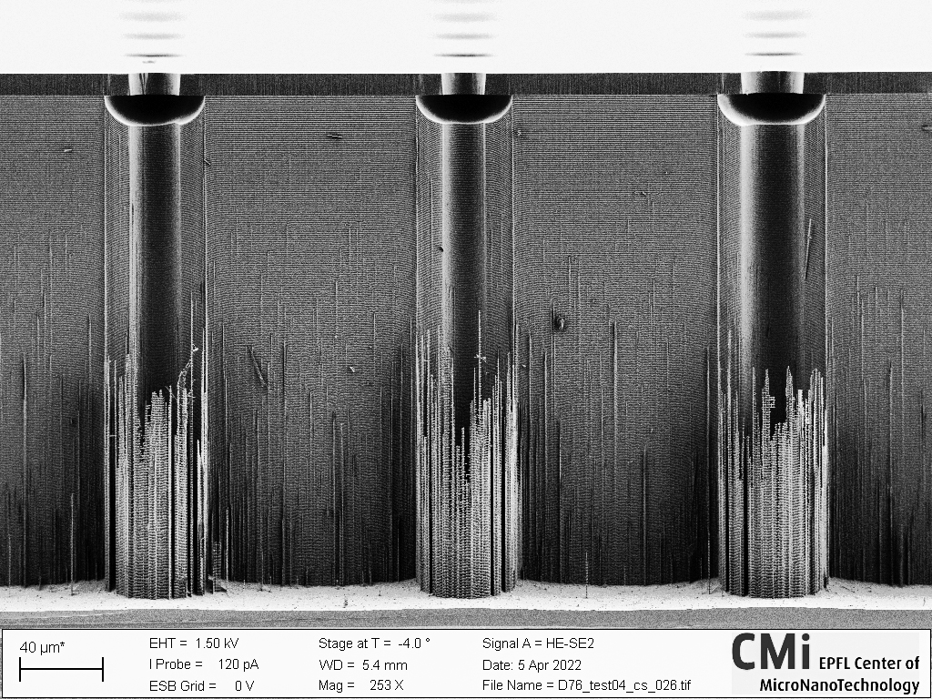
Silicon chimney stack
Rui Ning Wang, LPQM
An attempt at industrial landscape art using cross section SEM of SiO2 suspended structures obtained by undercutting the Si below with XeF2. The cross section was then obtained using a second photolithography and deep Si etch via Bosch process. During that process, photoresist residues stuck in the undercut area might have caused micro-masking, creating the tall fence-like structures.
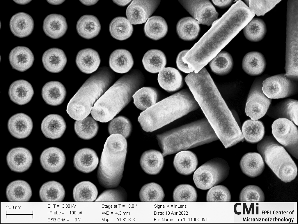
Nano cigar box
Tao Jiang, NAM
Box of nano cigars made of TiO2. The nano cigars have been drawn out randomly.
Platinum cell culture
Francesco Bertot, HYLAB
Who knew that cells can be made of platinum? The effect of heat during platinum deposition is sufficient to create air bubbles that resemble living cells. Some of them even seem to be in the middle of mitosis, maybe a new frontier in biology?
2022, March
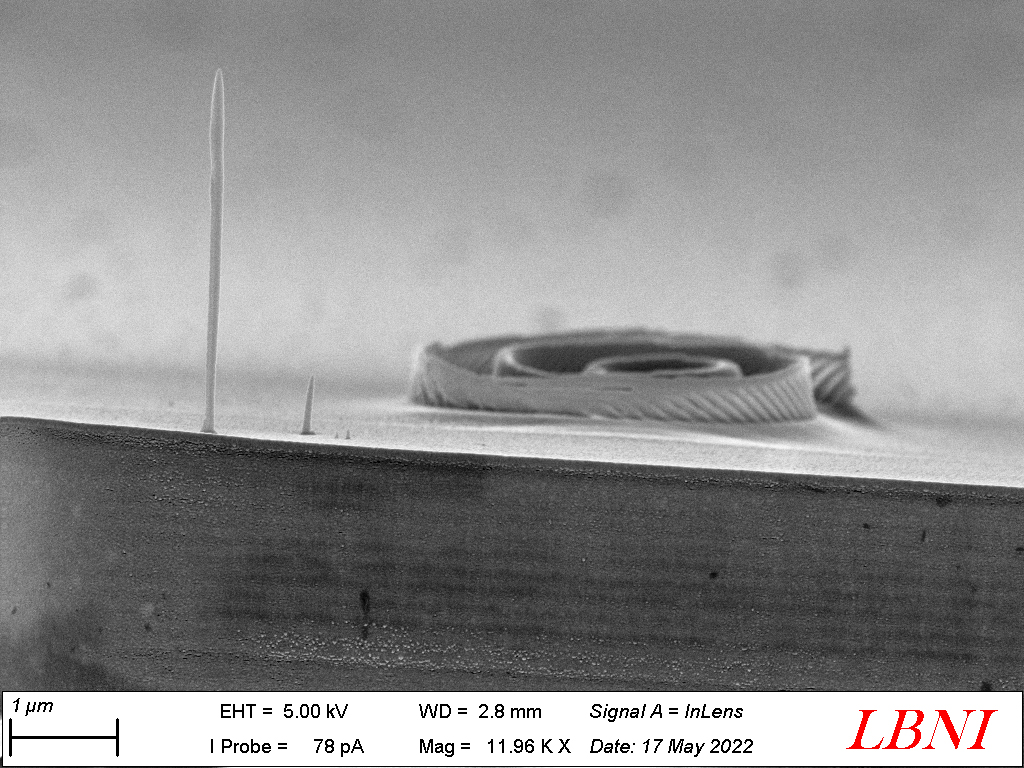
Totems
Alberto Beccari, LPQM
Grab one of these, get used to its feel and weight. Spin it to know without a doubt that you’re not in someone else’s dream (Inception, 2010). These silicon nano-pillars have been over-etched for too long with DRIE, causing notching at the base. The steam is then easily undercut with hydrofluoric acid, causing the pillars to fall on their side.
Inorganic dumplings
Alberto Beccari, LPQM
After a sleepless night and a developing a mild carpal tunnel syndrome, we managed to roll up thousands of baozi. Throw them in the steamer before the guests arrive. Cylindrical silicon nano-pillars have been covered with a silicon nitride film, grown with PECVD. The deposition is not quite conformal, giving the impression of inflated, tasty nanobuns.
Golden Star Wars are taking place at CMI
Francesco Bertot, HYLAB
It seems emperor Palpatine has ordered the construction of a new death star! Luckily, the rebels are already preparing an attack with a series of golden bow-tie fighters, ready to come out from the clouds. This result has been obtained after E-beam lithography and titanium-gold evaporation. Bad adhesion of the metals over the resist caused the formation of air bubbles and the peeling off of the deposited layer.
2022, February
Pushing towards the resolution limits
Franco De Palma, HQC
On a 2-dimensional hole gas originated in a SiGe/Ge heterostructure, quantum dots (QDs) are defined by 25-30 nm Ti/Pd gates patterned through the combination of e-beam lithography, evaporation and lift-off. In the upper part, a single QD used as a single hole transistor faces one of the two QDs used as qubits, the fundamental blocks of quantum processors.
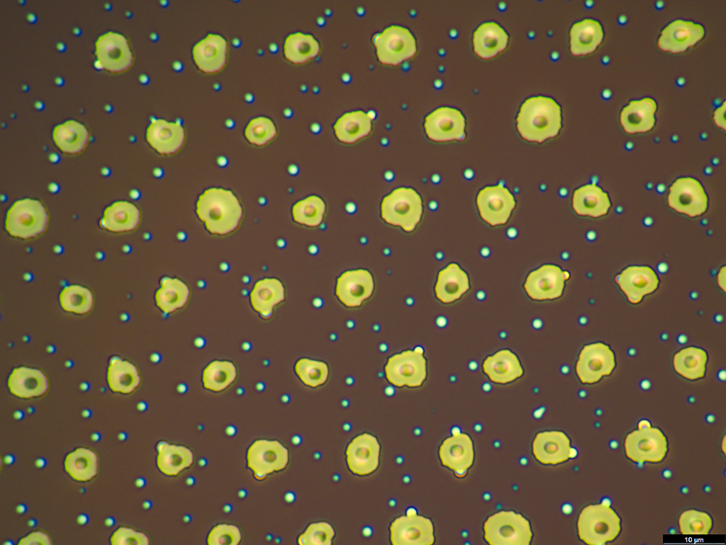
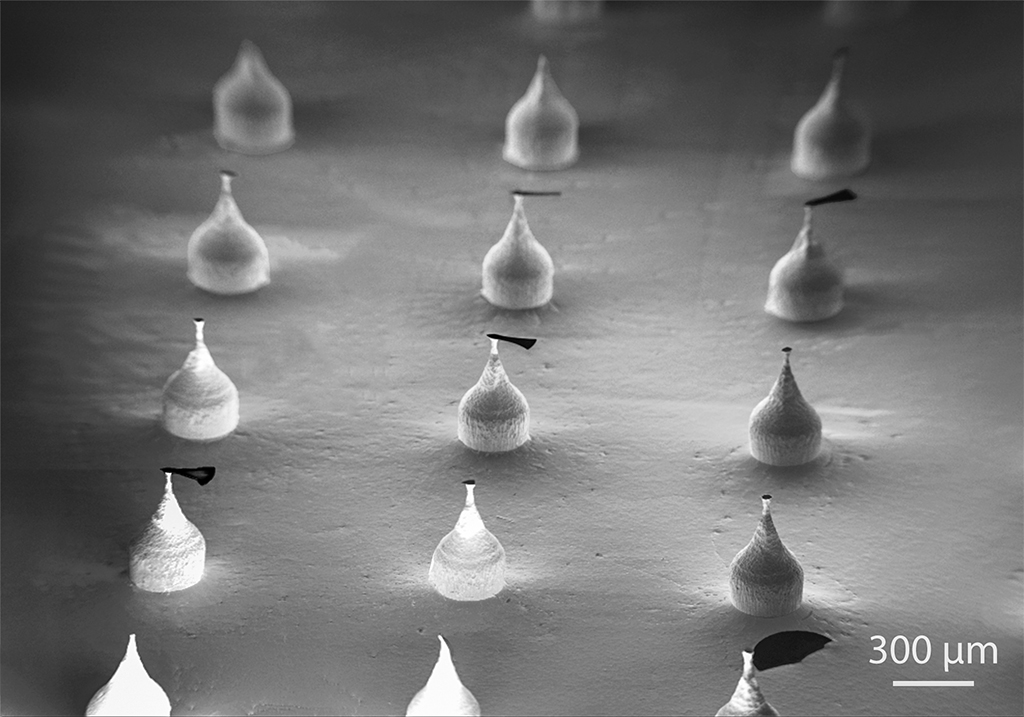
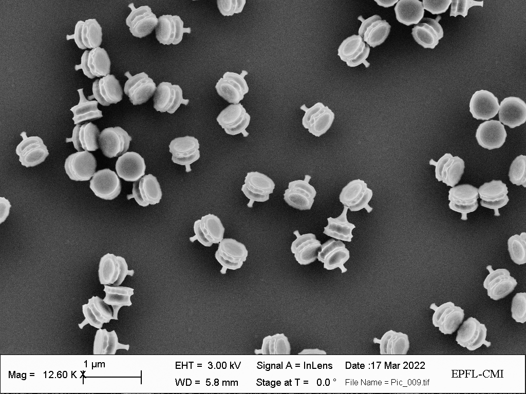
Belated Merry Christmas!
Marco Riccardi, NAM
By exploiting surface and capillary forces, a single 60 nm gold nanoparticle is delivered inside each of these holes milled in the gold substrate with the aid of FIB. The result is an array of nano-Christmas trees, which can potentially be used as a template to help assembling the particles.
Spider on a Brick Wall
Rajrupa Paul, Valerio Piazza, LMSC
Micro-cracks formed on monocrystalline Zn3P2 thin film. The challenge is to not place the hall bar on these cracks.
Goldfish
Hung-Wei Li, Nanolab
After the deposition of metal, buffer layer, and catalyst in CMi, dense carbon nanotube forest grew on the substrate. We wanted to observe the surface after measurement, and we found a goldfish swimming on top of the carbon nanotube forest!
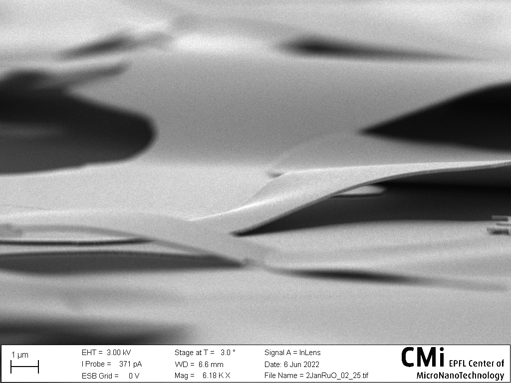
Micro black hole
Pierrick Clément, LMIS1
A broken SiNx/SiO2 membrane revealed the back side of the Si wafer that was etched by the Bosch process.
2022, January
Birth of Batman
Viacheslav Snigirev, LPQM
Area around electrode pads drawn by an electron beam in a double layer of 500 nm of MMA / 500 nm of PMMA coated with 30 nm of Al. Exposure with a dose of 1600 uC/cm2 and a beam current of 100nA on a Si substrate with 2um oxide layer generates enough heat to cause the conductive protective Al top layer to crack, buckle and eventually burst open.
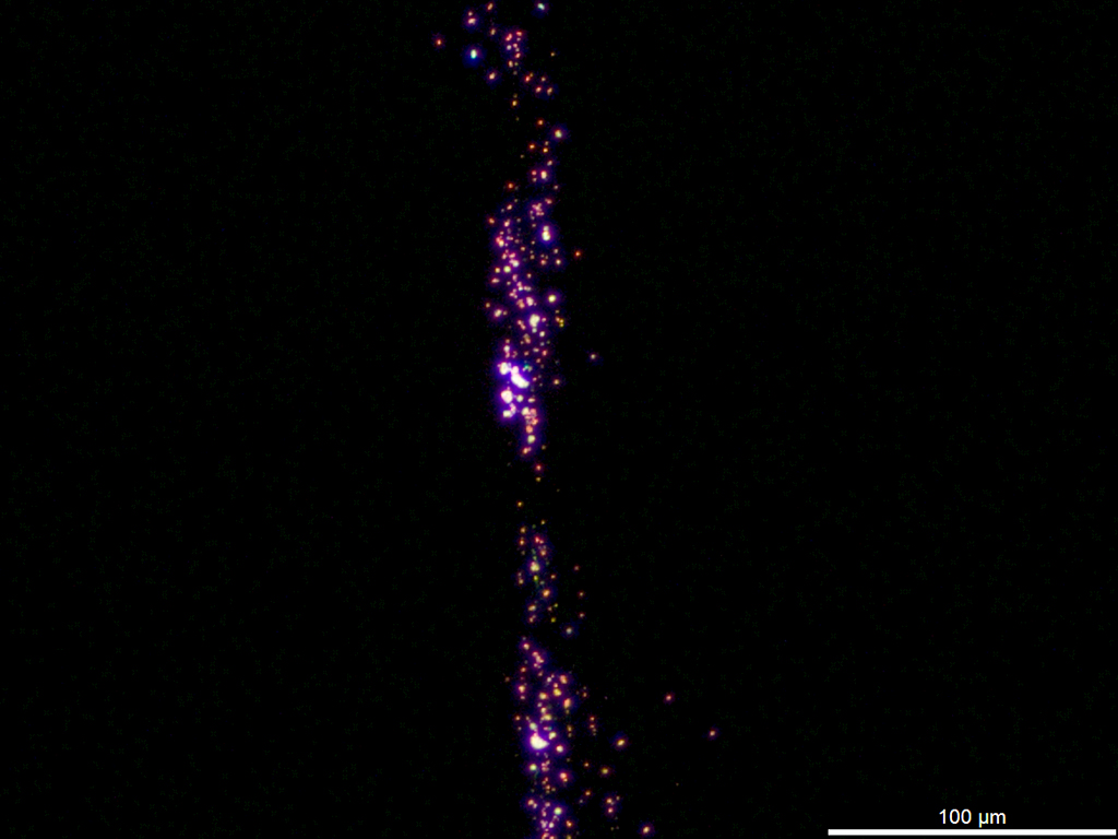
Milky Way
Stephan Gamper, Miraex
Dark Field microscope image used to spot scratches and residues on the surface.
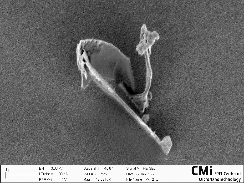
A micro fawn
Veronica Leccese, LUMES
A micro-fawn in an aluminium field.