Restrictions and Precautions
2. When the system is not used, a dummy wafer should be loaded inside to avoid substrate holder contamination.
1. Maximum allowed booking per person between 9am and 5pm is 2 hours. It is still possible to get 4 consecutive hours from 7am to 11am or from 3pm to 7pm.
2. Reservation names must correspond to operators.
Contents:
- Introduction
- Equipment description
- Standard processes
- How to use the system
- References and photos gallery
I. Introduction
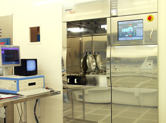
Adixen AMS200 etcher is an optimized Deep Reactive Ion Etching (DRIE) system for Silicon (Si) and Silicon on Insulator (SOI) wafers.
- Some special hardware arrangements make all these processes possible:
- A high density plasma sources: Inductive Coupled Plasma (ICP),
- A temperature controlled process chamber,
- An Electrostatic Clamping Chuck (ESC) controlled in temperature for wafer cooling,
- Two possible wafer voltage biasing: RF (13.56MHz) for dielectric etching and pulsed Low Frequency (LF) for Si etching,
- A powerful gas process pumping arrangement (Adixen 1600l/s Turbo pump + Adixen ADP122 rough pump).
- Processes can be separated in 3 families:
- Si etching with pulsed process (Bosch process) and pulsed LF wafer biasing,
- Si etching with none pulsed process (continuous process),
- Dielectric etch with RF wafer biasing.
Major advantages on this system compare to older generation one are:
- Wafer voltage biasing choice (RF or pulsed LF),
- Process chamber heating to limit polymer contamination and for a better processes reproducibility. In principle, no mechanical cleaning is necessary.
II. Equipment description
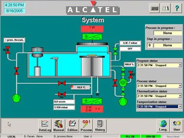
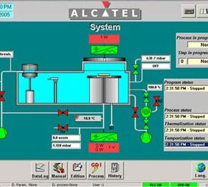
Graphic User Interface
AMS200 is totally driven through a very intuitive Graphic User Interface (GUI) with a touch screen. Figure 1 shows an example of process edition.
Wafer Loadlock
Loadlock and transfer arm are designed for fast transfer from loadlock to processing chamber (40s), and vice et versa.
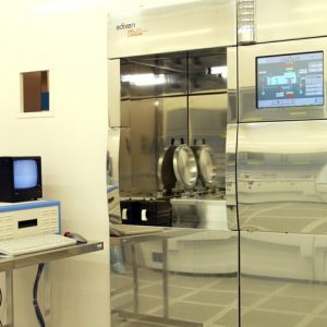
Processing Chamber
Figure 2 shows a global view of the AMS200 processing chamber. Main parts are visible: ICP source, diffusion chamber and ESC. End Point Detection (EPD) based on laser interferometry is performed through the viewport placed on the top of the chamber.
ICP source
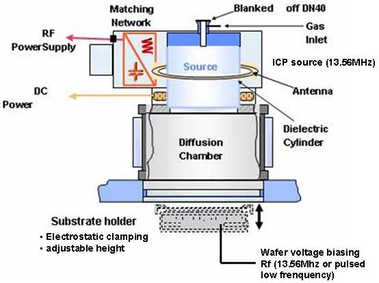
ICP source is made with an antenna connected to an RF power supply and wrapped around an alumina cylinder. RF power (13.56MHz and 3 kW maximum) is coupled to the plasma through an inductive mode. The oscillating current in the antenna at 13.56 MHz induces an electromagnetic field (E/B) in the alumina cylinder. For plasma ignition, some primary electrons collect the E/B field energy (ions are too heavy to get the energy from E/B field). Inelastic collisions between hot electrons and neutrals (injected gas mixture) give ions/electrons pairs. This is the way how the main plasma is created inside the cylinder where the gas mixture and pressure are controlled. A coil surrounding the plasma source gives a permanent magnetic field for a better plasma confinement and to avoid wasting too much charged species.
Diffusion chamber
Diffusion chamber is a buffered zone to get a better plasma uniformity. Permanent magnets surrounding the chamber limit charged particles wasting on the wall and keep a better plasma density. A heated liner inside the chamber limits polymer contamination and makes O2 plasma very efficient to clear polymers in case of extreme chemistry use. A better process reproducibility is also given with the liner.
ESC and substrate holder
The substrate holder (SH) is placed in the diffusion chamber. SH height is adjustable between 120 and 200mm. Temperature can be adjusted between -10°C and +40°C. Energy transfer between wafer and the chuck is insured by an He film applied between the wafer backside and the chuck. He pressure ca be set between 3 and 15mb.
Average ions energy is controlled through SH voltage biasing. It could be a pulsed LF voltage biasing (600 W maximum) or RF voltage biasing (13.56 MHz – 500W maximum). Correct biasing mode is automatically selected by AMS200 when a recipe starts.
Pumping
The combination of 1600 l/s Adixen turbo pump and Adixen ADP122 rough pump gives a secondary vacuum of few 10-7 mb without process. In process, the powerful pumping capacity makes possible the use of high gas flow (500sccm) at a low pressure (few Pa).
Gaz lines
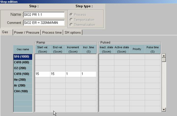
7 Mass Flow Controllers (MFC) and 6 different gases are available:
- SF6 [0-1000 sccm] – fast MFC
- C4F8 [0-400 sccm] – fast MFC
- C4F8 [0-100 sccm]
- CH4 [0-100 sccm]
- O2 [0-100 sccm]
- Ar [0-200 sccm]
- He [0-200 sccm]
SF6 [0-1000 sccm] and C4F8 [0-400 sccm] can be used in pulsed mode for Bosch process.
EPD
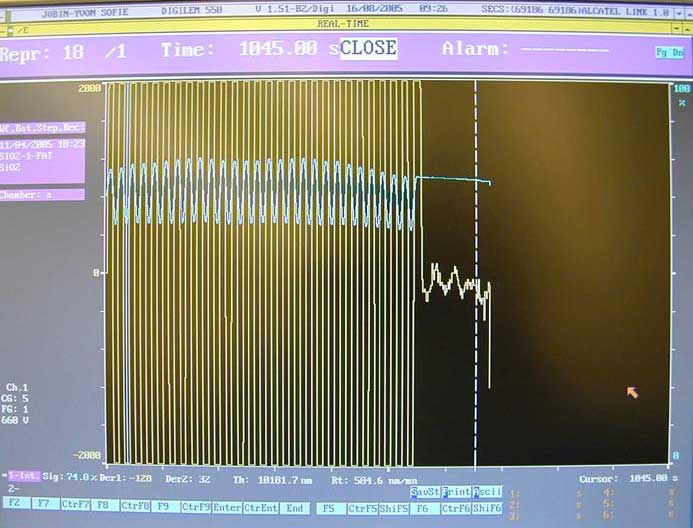
EPD based on laser interferometry is a non intrusive technique to measure transparent films (SiO2 or Si3N4) etch rate during process and to know when the buried oxide is reached during SOI etch. It also gives PR mask ER during etching. The principle is based on the 670nm laser intensity monitoring. Camera and laser are placed on a X/Y stage to accurately position the spot on the wafer. The laser spot is reflected on the wafer surface. During etching the transparent layer (PR or SiO2 for example) is thinned. It modulates the laser intensity since it gives constructive and destructives interferences. Figure 3 shows the results after a 9µm deep SiO2 etch. Blues lines is the reflected laser intensity and the red one is the first derivate . Average ER (504nm/min) and depth is displayed in live. Once SiO2 is completely etched, the laser is reflected on the Si surface and the intensity remains constant.
III. Standard processes
- Fused silica, Pyrex and Float Glass wafers need to be coated with a conductive layer on the backside because of the electrostatic clamping chuck.
- Edge Bead Removal (EBR) is not required in this system. It is even better to avoid EBR in case of deep Si etching because it makes the wafer thinner on the edge and it becomes fragile.
- Steps of “UNCLAMP” are used before unloading. They are aimed at removing residual ES forces to allow safe and successful wafer unloading. Please let the system unload automatically the wafer at “UNCLAMP”, do not abort or skip these steps. If you need to stop a process, hit “next step” until you reach “UNCLAMP” and let the tool handle the unloading. Do not hit “stop process” !
| Material | Substrate holder temperature (°C) | Process name | Mask material | Selectivity to mask | Material etch rate (um/min) | Remarks |
|---|---|---|---|---|---|---|
| Si – Bosch process / vertical etch | 30 | SOI_accurate: 5- (SF6 4.5s) 4- (SF6 5s) 2- (SF6 6s) 1+ (SF6 6.5s) 2+ (SF6 7s) 4+ (SF6 8s) | PR SiO2 | > 75:1 (PR) > 150:1 (SiO2 ER = ~ 20 nm/min) | 3 to 4.5 depends on design | Process optimized for SOI wafers to avoid notching. Process adapted to bulk Si wafers. Process given low Aspect Ratio Dependent Etching (ARDE). |
| Si – Bosch process / vertical etch | 0 | SOI_sharp | SiO2 | > 20:1 | 0.5 to 2 depends on design | Process optimized to get high Aspect Ratio (AR) up to 50. |
| Si – continuous process / vertical etch | 20 or 0 | Si_opto Si_opto_HR_20deg Si_opto_HR_0deg (nano) | PR SiO2 | > 10:1 > 20:1 | 0.2 to 1.2 depends on design | Process with slow ER adapted for shallow and accurate etch for less than 5um deep |
| Si – continuous process / isotropic etch | 20 | Si_release | PR Al SiO2 | > 100:1 > 500:1 > 200:1 | ~ 2 in lateral ~ 4 in vertical depends on design | Process designed for isotropic etching of silicon. |
IV. How to use the system
- Login on the AMS200 on zone 2 computer.
- Login on AMS computer (username:1, password:1).
- IDLE mode:
- A wafer is already loaded in the system to prevent chuck contamination and the IDLE process should run.
- Stop IDLE process and unload the wafer.
- To vent the loadlock, hit Ok when the window “End of Process” appears.
- Open the loadlock lid and put the dummy in the black box.
- Select the process according to your runcard and check steps and etching parameters:
- A process is made of different types of steps: thermalization, temporisation, etching and unclamping.
- Go to “edition” and select the process in the right list. Make sure the process contains at least thermalization (Therm XX with XX the desired temperature ) and temporisation (Tempo) as the first step and UNCLAMP 20MB and UNCLAMP-AR-20MB (in this order!) as the final steps. If not, add these steps. Select the etching steps and hit “modify” to edit. Standard processes are locked and etching time is the only accessible parameter.
- Start you first etch:
- Before loading the wafer, check the cleanness of the wafer backside. Very often after automatic development on Rite Track or on EVG150 or ACS200, it contaminates the wafer backside with developer. Wafers must be rinsed in DI water right after development.
- If the wafer backside is clean, load it in the AMS200 loadlock (front side up) and close the lid,
- Hit “Go process”, select the etching process in the scroll list and hit “Go run”. During the temporisation (20 or 30s wait to get the backside He cooling film), it is possible to move the camera and the laser dot by hitting “ctrl + arrow ” on the EPD keyboard.
- During “tempo” step, a wait of 30s, He backside pressure is applied. He leak should be in the range 0.5 to 1.5sccm and He pressure above 9.2mbar.
- If an etching process needs to be aborted WITH unloading of the wafer, hit “Next step” icon until you reach the UNCLAMP 20MB step and let the machine automatically unload.
- If an etching process needs to be aborted WITHOUT unloading of the wafer,hit “Stop Process” and let the wafer in.
- If the UNCLAMP 20MB + UNCLAMP-AR-20MB steps do not allow unloading of the wafer, hit the “Green light” icon to resume the step. If it does not help after 2-3 times, call CMi staff.
- Unload the processed wafer, check if the etching is good and keep etching the rest of your batch.
- Before leaving the system :
- Load a dummy wafer and start IDLE process. DO NOT stop IDLE process.
- Perform AMS200 logout on zone 2 computer.
V. Metrology
Optical microscope
- Specific vernier observation after etching give a good idea of the anisotropy
- Bottom etch observation tells if there is some roughness
- Depth is measurable by focusing on the bottom first, resetting the zero of the optical microscope fine adjustment tool and focusing on the top of the sample. The measurement accuracy is 1µm.
Mechanical profiler
Mechanical profiler in zone 4 (alpha-step) gives accurate step measurements in the range 0.1µm to 2mm. The system doe not work for when the aspect ratio becomes to high. The stylus cannot reach the bottom.
Interferometry
Spectro-reflectometer (Nanospec) in zone 3 gives accurate thickness measurements for transparent layer (SiO2 ou Si3N4 for example) on Si. This metrology is not suitable for thickness less than 10nm.
Scanning Electron Microscope (SEM) and Focus Ion Beam (FIB)
SEM is a very powerful tool to study profiles after etching (verticality, roughness, depth, selectivity…). It is very often necessary to cleaved wafer to get a full etching characterization. When it is not possible to destroy the wafer, a local cross sectioning can be performed with FIB.
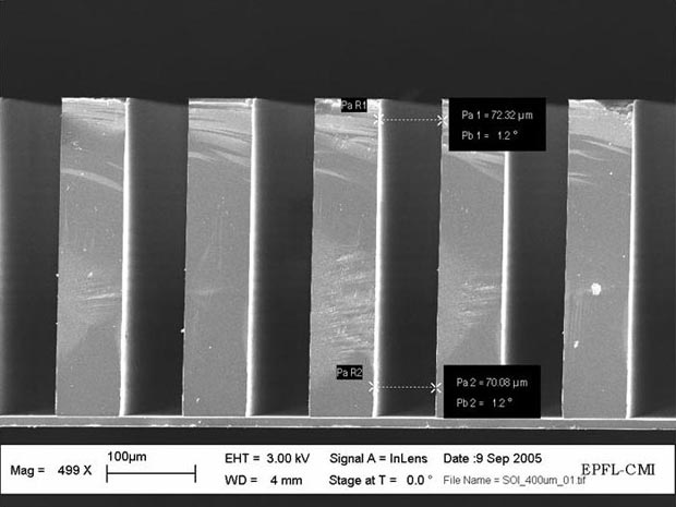
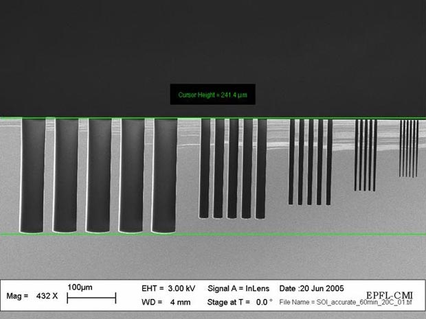
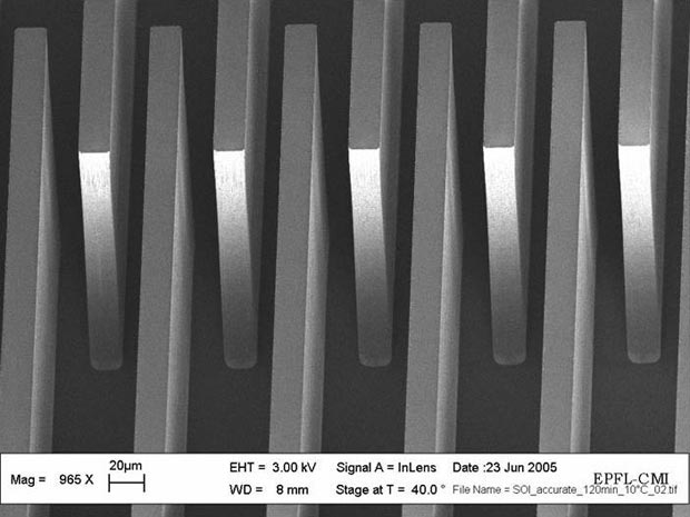
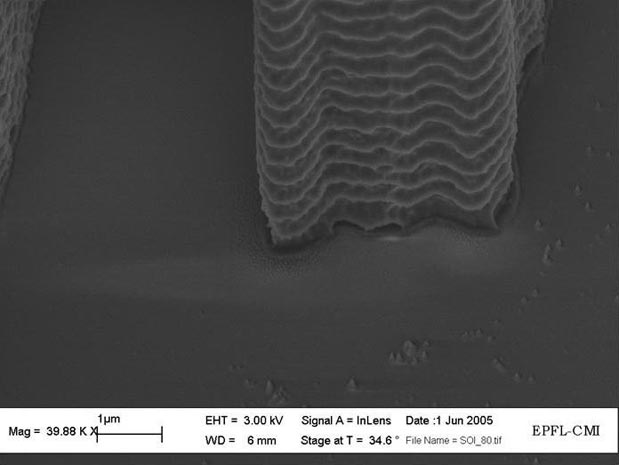
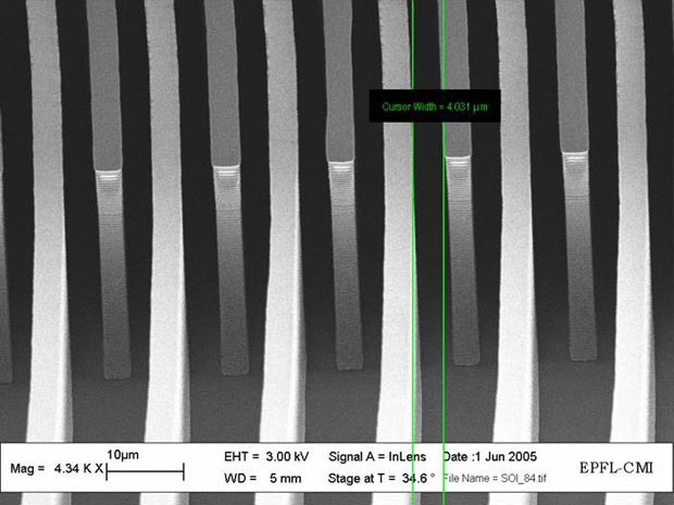
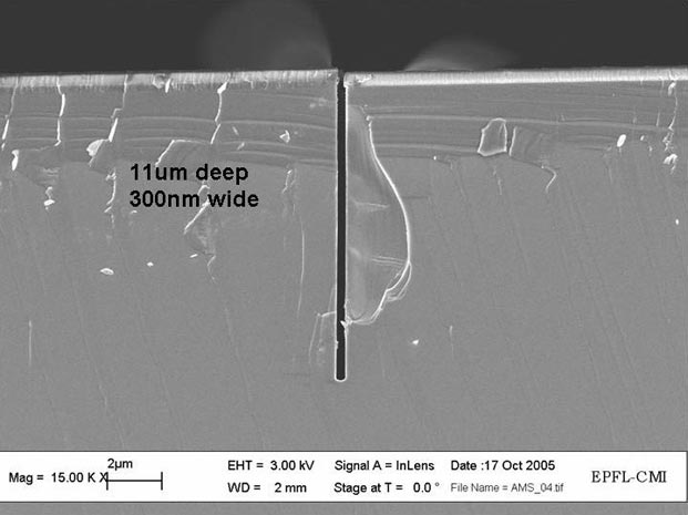
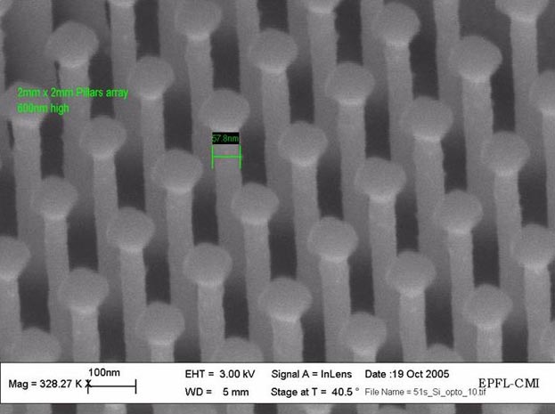
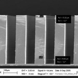
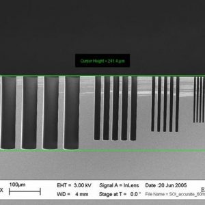
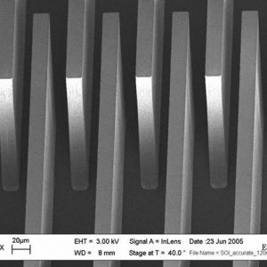
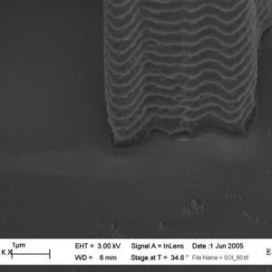
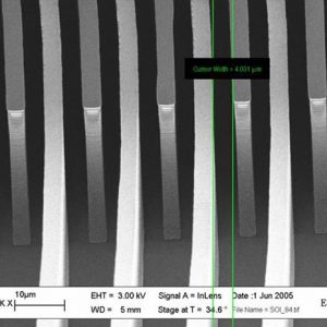
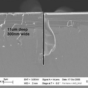
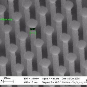
VI. References et photos gallery
1 C. Hibert and Ph. Flückiger, “Deep anisotropic etching of Si using low pressure high density plasma. Presentation of complementary techniques and their application in microtechnology”, ISPC 15 (International Symposium of Plasma Chemistry), Orléans, june 2001.
2 M. Pavius, C. Hibert, Ph. Flückiger, Ph. Renaud, L. Rolland and M. Puech, “<a href="https://cmi.epfl.ch/etch/MEMS2004.pdf" title="Profile Angle Control in SiO2 Deep Anisotropic Dry Etching for MEMS Fabrication” class=”cmi_manual” style=”font-family: ‘Times New Roman’;font-size: medium;font-style: normal;font-weight: 400;letter-spacing: normal;text-align: start;text-indent: 0px;text-transform: none”>Profile Angle Control in SiO2 Deep Anisotropic Dry Etching for MEMS Fabrication” MEMS-04 Maastricht.