Ebeam lithography at 100kV can only be performed on electrically conductive substrates, or on substrates coated with a thin conductive layer of metal properly grounded to the sample holder.
The schematic drawing below illustrates some of the most common grounding schemes, as well as several of the most likely mistakes. The principle is simple – there must always exist a conductive path for the incident electrons to travel all the way to the sample holder, which itself is properly grounded by the tool. Any non-conductive obstacle will result in charging problems.
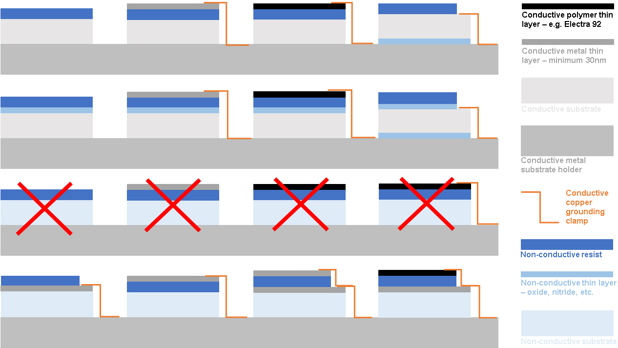
The energy in the lithographic electron beam can be as much as million times higher than it is on the SEM set up to image poorly conductive samples. Trouble starts if this energy does not have a chance to be properly and immediately dissipated. The severity of the problem and its consequences will depend on the actual setup. They can be relatively mild, but there exists a serious potential for a physical damage to the tool and several weeks of downtime.
How bad can things get?
Relatively good scenario – small charging
Even in cases where everything was setup correctly, small amount of charging can be present. Most ebeam resists are insulators, and if they are the top surface layer, however thin, some charging will happen there. Depending on the resist, current, pattern density, writing speed and writing order, several nanometers or even tens of nanometers of beam displacement and pattern placement errors can result. The mask-making industry had to introduce conductive polymer top-coat and other writing order modifications already around 65nm technology node for certain mask designs to meet the ITRS roadmap image placement specifications.
Bad scenario – strong charging
When charging gets stronger, the lithography suffers. Image placement errors become noticeable, commonplace, and often the patterns disappear altogether as the beam gets deflected by the strong surface charge. Here is an example of what can happen during an exposure on a non-conductive substrate with properly deposited thin metallic layer, that unfortunately failed to get grounded properly. Substrate – glass, coated properly with thin layer of Ti+Al, resist HSQ.
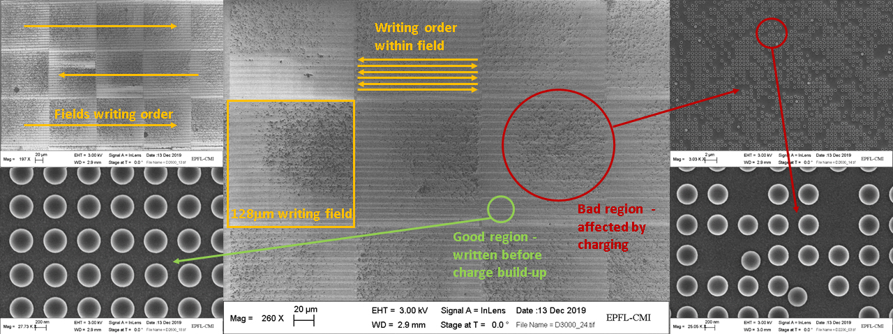
The thin conductive film got saturated with charge very fast, and once it did, the resulting charge deflected the beam all over the writing field. The charge only got a chance to dissipate little bit during the field-to-field stage move delay, resulting in a repetitive pattern of disorderly lithography. Image courtesy of Karim Achouri and Kevin Mueller.
Catastrophic scenario
If one simply coats a glass substrate with a polymer resist and starts an exposure with high enough current, dense pattern and high enough dose – really bad things will happen really fast. The massive accumulated energy will instantly increase the substrate surface temperature above the resist melting point, there will be an explosion of micro-droplets of resist into all direction. If one of those droplets finds its way into the objective lens, it will be game over for any lithography, as the beam will now charge and drift, until the column gets opened and cleaned (all affected parts replaced) – potentially several weeks of downtime.
In case the substrate is not only insulating, but also pyroelectric (for example lithium niobate), there also exists a potential for some of the detectors and electronics inside of the tool being knocked-out by an induced surface discharge.
The ability of the tool to generate large amount of heat very rapidly even in a properly metal coated and relatively thin non-conductive layer on top of an otherwise conductive substrate is illustrated in the example below.
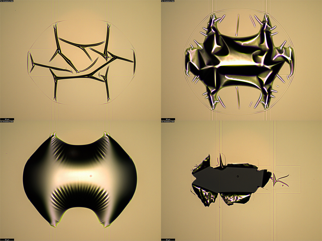
Area around electrode pads drawn by an electron beam in a double layer of 500 nm of MMA / 500 nm of PMMA coated with 30 nm of Al. Exposure with a dose of 1600 uC/cm2 and a beam current of 100nA on a Si substrate with 2um oxide layer generates enough heat to cause the conductive protective Al top layer to crack, buckle and eventually burst open. Image courtesy of Viacheslav Snigirev.
Short note about metal processing
Metal deposition
For metal deposited below the resist, any metal and any deposition tool compatible with the rest of user’s overall process flow can in principle be used. During resist coating, one must leave a small area of the metal uncoated, in order to have an exposed metal layer available for the grounding pins (on 100mm holders) or for copper tape. The advantage of coating metal below the resist is the timing logistics. The metal can be deposited essentially any time prior to the resist coating, and on any deposition tool.
For metal deposited on top of the resist, only deposition tools that do not expose the substrate/resist to electrons can be used. At CMi, the least amount of electron exposure is achieved in EVA451 thermal evaporator, LAB600 ebeam evaporator and EVA760 ebeam evaporator. The deposition process also has to be sufficiently cold, as many of the ebeam resists have relatively low glass transition and melting points. The dis-advantage of coating metal on top of the resist is some exposure during the deposition and subsequent implication for image quality and size and the timing logistics. Metal can only be deposited after the resist coating, and on only a small subset of deposition tools listed above. Metal also has to be removed before the resist can be developed.
Metal removal
For metal deposited on top of the resist, the two common choices are Cr and Al. Al is typically used for processes with HSQ/FOX resist. It can only be coated of top of the HSQ/FOX, because the TMAH resist developer also acts as an etchant of the Al. Coating HSQ/FOX on top of aluminum will likely result in full lift-off during develop.
Chromium removal, 24/7 available, Arias Acid Bench in Z14
Aluminium removal if coated on top of HSQ/FOX resist, 24/7 available, Ebeam Base Wet Bench in Z7