EBPG5000plus ebeam writer requires sufficiently flat (<100μm) horizontally mounted substrate with an opaque and reflective surface.
The ebeam tool needs to know, where the surface of the substrate is, in order to properly focus the beam on it and to properly deflect the beam into a desired location on it. Any mismatch between the perceived surface height and the actual height inevitably results in both focusing and deflection errors. The larger the height position error, the larger the de-focus and image placement errors, see image below for the illustration schematic of why that is.
Focusing and image placement errors
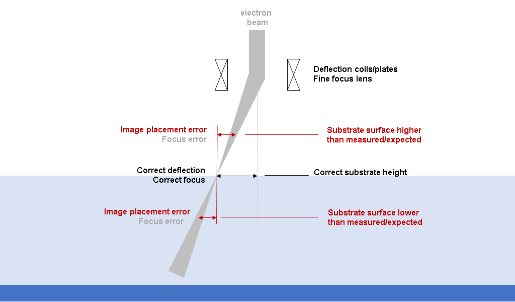
The ebeam tool can only deflect the beam within 250μm field. When the field is written, the stage with the substrate moves to a next field position. Any deflection error thus results in a pattern “stitching” error at the field boundary. If the real height is lower than expected height, the patterns from the neighboring fields overlap. This is the happier scenario. If the actual surface level is above the expected value, the deflection falls short of its target location, and a continuous pattern gets broken into two separate patterns at the field boundary. This results in a broken electrode, broken waveguide, etc. and basically a “trash wafer”.
In-situ surface height measurement
To minimize errors due to a wrong height information the EBPG500plus is equipped with an internal laser height measurement system, and the tool is setup to verify (measure) the substrate height every time the stage moves to a new field. Provided the measured height falls within a +/-50μm range from a set optimum, all deflections and fine focus are adjusted on-the-fly to compensate. If the height error falls within the +/-50μm to +/-100μm range, the tool is no longer able to fully compensate for this, but it will do its best, and it will continue to write with the understanding that the de-focus and stitching errors are going to be still mostly acceptable for most applications. If the measured height falls outside of the +/-100μm range from optimum, or if the height cannot be read, the tool will skip the writing field. This may result in substantial parts of pattern missing. But were those parts of the pattern written, they would be blurry, out of focus, and out of place. The tool does this in part to protect itself from blasting a high power electron beam over the stage outside of the substrate, should a user request by accident to write there.
Opaque and reflective surface
The use of laser beam to measure the sample surface position obviously requires that the surface is reflective. Excessive surface roughness, previous lithographic patterns (for example diffraction grating) that are optically active, and on a rare occasion even “stealth-like” surfaces (covered with poly-crystalline material with large enough randomly oriented facets – e.g. chrome deposited on top of PMMA in DP650 sputtering tool at CMi) – all of these obviously make the surface height measurement impossible to perform. In some circumstances, manual workarounds can be setup to enable writing on such surfaces provided the height has been pre-determined by other means and correctly entered into a writing job.
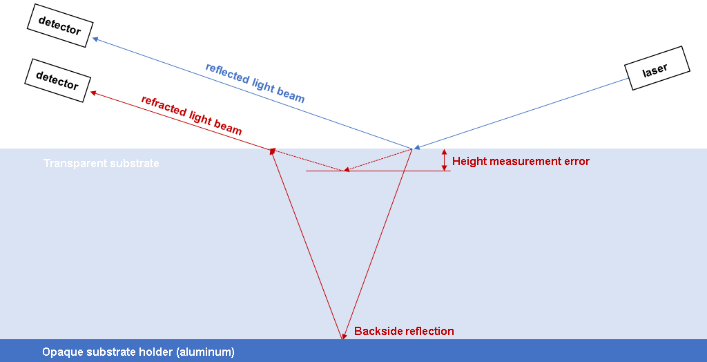
The need to measure height by laser light reflection also requires that the sample surface be opaque! If the sample is transparent, even though there maybe sufficient reflection from the top surface, there will also be a refraction of the laser light into the sample itself. On the backside, the light beam will reflect, both from the backside and from the opaque metal sample holder below the backside, and this reflected beam will find its way back up to the surface, where it will refract again, and it will thus trick the detector to perceive the surface height to be in a wrong place. On a regularly used thickness of wafer substrates, the error will be sufficiently large to destroy the lithographic performance, focus, image placement and stitching.
Correct and incorrect ways of sample mounting
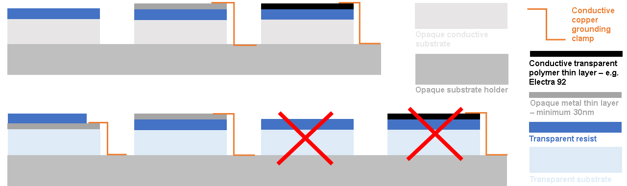
Anyone who wishes to write on top of a transparent substrate needs to first deposit at least 30nm of opaque layer on the top of the substrate. The opaque layer can be metal or silicon, and the opacity and thus the ability of the laser to correctly measure should be first verified using the alignment microscope in the resist processing room of zone 7. The reported height of the surface by the microscope should remain constant (or be only changing slightly but always smoothly) as one moves the sample around in X and Y direction. Any sudden jump in the height reading indicates most likely a refraction and back-reflection from the grooved substrate holder surface below the sample.
Word of warning – Electra 92, while appearing black in the bottle, is not opaque enough to serve as a reflective opaque coating. Wrong height reading will ensue.
Since most of the commonly used transparent substrates (glass, silica, diamond, niobate, etc…) also happen to be electrically non-conductive, depositing (and properly grounding) at least 30nm of metal layer is usually the best solution, as it resolves both the conductivity and reflective opacity problem.