F54 is an automated thickness mapping system manufactured by Filmetrics, a KLA Company.
The tool can be used to map thin-film thickness of samples up to 200 mm in diameter quickly and easily using an advanced spectral reflectance system. A motorized r-theta stages moves automatically to the selected measurement points and provides fast thickness measurement.
Measurement thickness range is 20 nm – 45 μm using light with a wavelength range 380-1050 nm. For thinner films requiring UV light switch to the Filmetrics F20-UV.
Content
1. Introduction
When light hits a translucent film, some of it is reflected from the top of the film, some other from the bottom, and some other finally goes through the film. Spectral Reflectance analyzes reflected light to determine the thickness and the optical properties (refractive index n and extinction coefficient k) of dielectrics, semiconductors, and thin metal films. As an optical technique, it is accurate, non-destructive, and requires little or no sample preparation. Compared to ellipsometry, spectral reflectance uses light that is reflected perpendicular to the film (thus mostly ignoring polarization effects).
The amplitude and periodicity of the reflectance of a thin film is determined by the film thickness and optical constants (plus other properties, among which roughness). During the measurement, film properties are determined by calculating reflectance spectra based on trial values of mathematical model parameters (thickness, n, and k) and adjusting these values until the calculated reflectance matches the measured one.
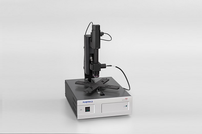
2. Equipment description
- Integrated Spectral reflectometer/Light source unit with fiber optic cables
- 5x and 15x objectives on a manual microscope adapter (C-mount fitting, 1 free position)
- High-speed r-theta polar stage with vacuum clamping
- NIST-traceable thickness standard (1000 nm SiO2 on Si) and Si wafer standard
- Through-the-lens camera for small feature measurement and/or alignment
- Spot size can be varied by changing measurement apertures (staff only). Installed size is 250 μm, 500 μm available on request.
- User-friendly software with extendable material library (supporting most common models as well as direct import of nk files ) and programmable mapping capabilities
3. Operation
- Do not touch or bend the fibers
- Keep hands away from the stage during operation
- Do not touch or scratch stage reference or background mirror
- Avoid crashing samples onto the objective (move to load/unload position (0, 100) )
Procedure to to take a single measurement on a sample:
- If you are the first user of the week, turn the lamp ON (tool is usually always ON)
- Switch To FILMapper software
- Move the stage to load position (x = 0 mm, y = 100 mm) and load the calibration sample (SiO2 on Si)
- Pick a the “SiO2 on Si” recipe (check the parameters are correct)
- Select the appropriate objective and choose the matching configuration in the software (important!)
- Take a baseline following the wizard
- Move to the (0, 100) mm position, unload the calibration sample, and load your sample
- Pick a recipe, edit the applicable parameters in the tabs (Stack, Analysis options, Wafer mapping, Acquisition settings)
- Navigate to the point of interest using the camera and r-theta controls (mind polar coordinates!)
- Hit Measure (check the goodness of fit)
- Unload your sample at (0, 100) mm position
Basic statistics on all measured data are available in the History tab (you can purge the database). Data can be exported in spreadsheet format.
Wafer mapping can be achieved by starting the measurement from the Wafer mapping tab (warning: wipes history cache). Maps can be exported from the File menu.
Refer to the user manual for details about the baseline procedure (including an important adjustment and common error troubleshooting).
4. Tool specifications
[1]: material- and objective-dependent
[2]: available on request