To be read first:
- Wafers and photoresists exposed on the MJB4 must be accepted by the technical comittee. CMi staff approval is required before using any non-standard products.
-
Cross-Contamination: Samples must be free of backside contamination. Mechanically unstable metal layers (delamination) are not allowed. Note: a special chuck is available for use with PDMS coated wafers. Please ask the CMi staff for guidance.
-
Mask should be checked after each working session. Clean with acetone / IPA or with soft tissue to remove any solid or liquid residues.
- Please immediately inform the CMi staff in case of problems with the equipment.
RESERVATION RULES AND BOOKING FEES POLICY:
- No booking restrictions.
- 24/7 booking/use is possible with CMi+1 extended access.
- Reservation names must correspond to operators.
Contents:
I. Introduction
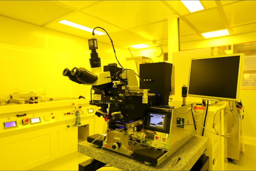
The MJB4 is a mask/wafer aligner for research and development, designed to align and expose wafers up to 4 inch (100 mm) diameter. Wafers, coated with photosensitive resists (PR), are exposed through a glass/chrome mask using a short (few seconds) pulse of UV radiation from a mercury (Hg) lamp, with spectral lines at 365nm, 405nm and 436nm. The illumination configuration is i-line (filter installed), meaning only the 365 nm spectral line is absorbed by the resist.
The parallelism between the wafer and the mask is achieved with a semi-automatic procedure of Wedge Error Compensation (WEC). Alignment is achieved with manual micrometer knobs down to a precision of about 0.5 µm. Only the top side alignement option is available.
The resolution is limited by light diffraction through the mask opening, and can reach a minimum of about 800 nm with thin PR thickness (< 1 µm).
II. Equipment description
Configurations:
MJB4 (Mask Aligner)
The MJB4 is a mask to wafer alignement and exposure system. One alignment modes is available: Top side alignment (TSA). The MJB4 is equipped with several options for fine handling of small wafers/chips.
Default illumination setup for exposure: 20 mW/cm2 @ 365 nm (i-line).
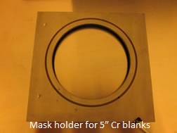
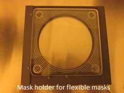
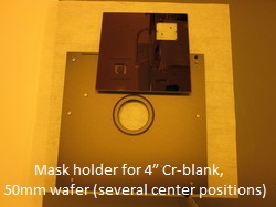
Mask holders:
Three different mask holders are equipped with vacuum clamping:
Available chucks:
Three different chucks for all sizes:
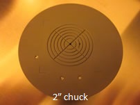
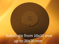
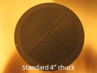
Note: chucks can be used for wafer/substrate thicknesses from 0.1 mm up to 4.0 mm.
Small wafer/chip objectives:
MJB4 is equipped with offset objectives for alignment of small wafer/chips. Minimum separation is 10mm.
Technical Caracteristics:
- Hg light source with deep UV cutoff (No quartz optics!), default illumination setup: 20 mW/cm2 @ 365 nm (i-line filter installed).
- Topside (TSA) alignment, using splitfield mode (two objectives).
- Exposure modes are flood-exposure, proximity, soft contact, and hard contact.
- Objectives magnification: 5x, 10x
- Special offset objectives for chip alignment (separation distance down to 10mm).
- Alignment using fine adjustment screws (alignment accuracy about 0.5µm).
- XY table movements : X = ± 30 mm Y = ± 30 mm Θ = ± 4°
- Manual substrate handling up to 100mm diameter.