1. Sample dimensions: The EVG bonding line (all four tools) are configured for the preparation and bonding of 100mm or 150mm wafer stacks. Chip to wafer bonding is not possible on this equipment.
2. Wafer surface cleaning: The surface of wafers processed in the EVG 510 bonding chamber should be as clean as possible. Having a smooth, particle-free, defect-free surface is extremely important to achieve reliable and good bonding results, free of voids and cracks. Make sure to transfer wafers to the bonding equipment rapidly after your cleaning sequence (RCA, piranha, plasma activation, megasonic DI water cleaning)
3. Bonding process method: The design of the EVG 510 bond chucks and pressure plates are different based on the bonding process method (anodic, direct or with intermediate glue). Make sure to correctly indicate your bonding method when booking the tool, and respect the configuration planning.
4. Please immediately inform the CMi staff in case of problems with the equipment.
1. Booking and configuration request of the EVG 510 are mandatory.
2. Reservation names must correspond to operators.
3. Configuration are potentially changed 2 times per day (morning: 7h-8h, afternoon: 13h-14h).
4. Extended access to the tool (19h – 22h) can be granted exceptionnaly to start overnight jobs.
5. Current booking limit: Single user –> 12 slots, group –> 24 slots
Contents:
I. Introduction
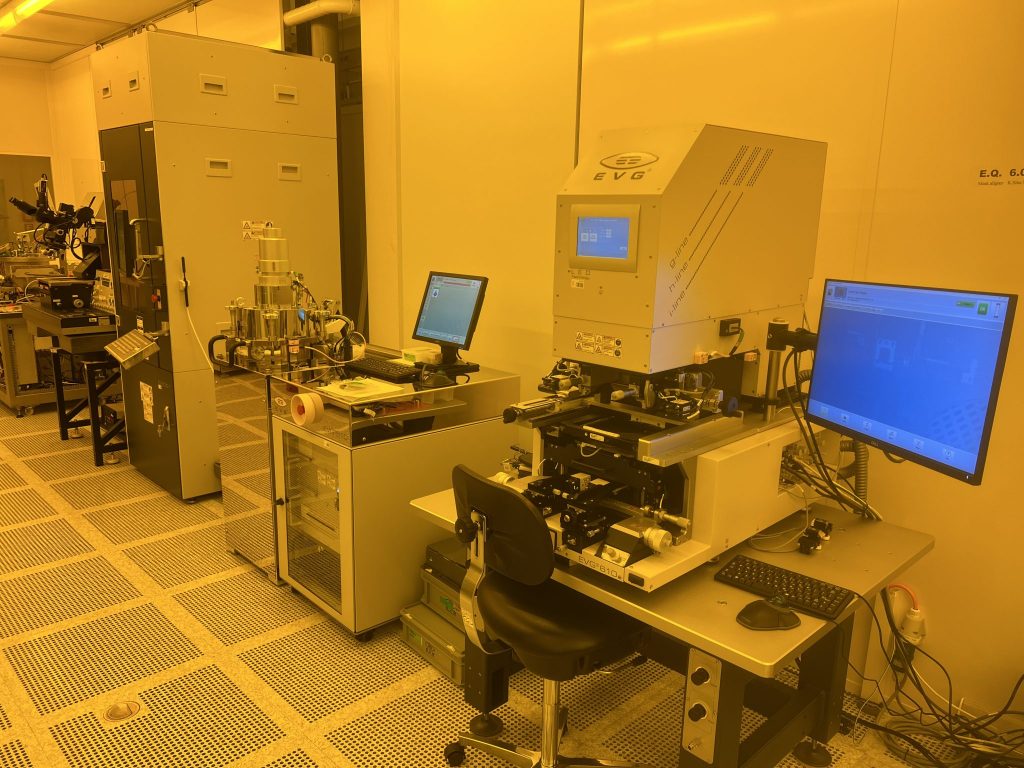
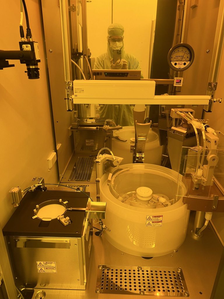
The wafer bonding line from EVG is a set of 4 processing equipment entirely dedicated to the surface preparation (cleaning and activation), alignment and bonding of 100mm or 150mm wafer stacks :
- EVG 810LT, low temperature plasma activation system (N2, O2, Ar): The EVG 810LT is used to activate the surface with a plasma treatment to promote the formation of bonding sites. The recommended gas chemistry for the treatment depends on the wafer surface material.
- EVG 301, DI water megasonic wafer cleaning system & pre-bonding station with IR inspection: The EVG 301 is used to clean wafers with DI-water using a megasonic brush that scans the whole surface. In addition, it features a station to contact wafers that directly bonds together (flat-to-flat alignment), and an infrared illumination/camera module to image the bond interface and detect the presence of voids.
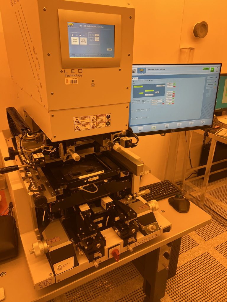
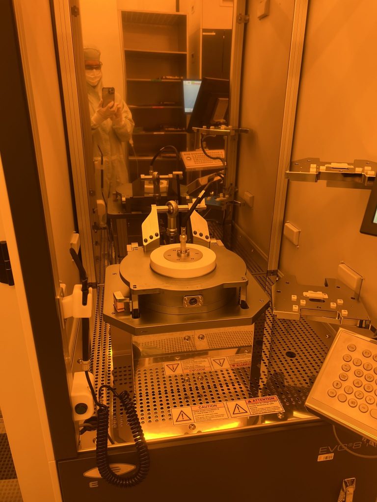
- EVG 610, bond (and mask) alignment system, with silicon direct bond (SDB) option: The EVG 610 bong aligner is used when critical alignment is needed between the bonded wafers. Two operating modes are available: 1) EVG 510 bond chuck preparation –> wafers are aligned and mounted on the EVG 510 bond chuck for further processing into the bonding chamber; 2) Silicon direct bond (SDB) –> Used with wafers that directly bond together (direct bonding): Wafers are aligned, pushed in contact for direct bonding, and the stack is unloaded from the slide.
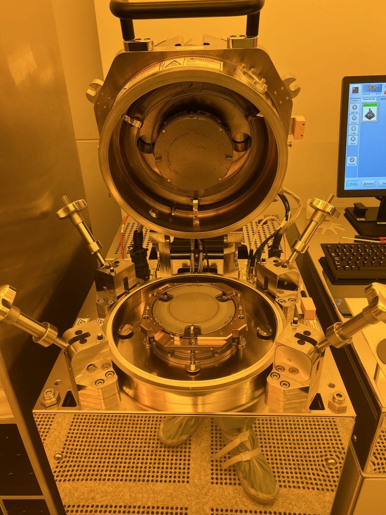
- EVG 510, wafer bonding system (anodic, direct or adhesive): The EVG510 is an equipment for bonding wafers. The bonding chamber process parameters are: 1) temperature of the pressure plates, 2) tool pressure applied on the stack of wafers, 3) chamber vacuum pressure and, 4) bias voltage applied between the plates. The system is compatible with most of the standard low-temperature bonding methods (anodic, adhesive, direct).
The EVG 510 bonding chamber can be configured with different sets of toolings (wafer chuck, fixture, pressure plates, electrodes, etc…) allowing to perform bonding with most of the popular bonding methods such as:
- Direct bonding (with or without surface activation)
- Anodic bonding
- Eutectic bonding
- Glass frit bonding
- Adhesive (glue) bonding
- Thermocompression bonding
The bonding sequences of the EVG 510 can be fully edited to adjust the following parameters:
- Chamber pressure set point (N2 ambiant), down << 1E-04 mbar (turbo pumping).
- Temperature set point and ramp speed, up to 550°C (independant setting for top and bottom pressure plate).
- Tool force up to 10kN.
- Voltage bias up to 1000V.
Conventional, silicon to silicon “fusion” bonding, that requires temperature > 800°C, cannot be achieved directly in the EVG 510 bonding chamber.
II. Equipment description
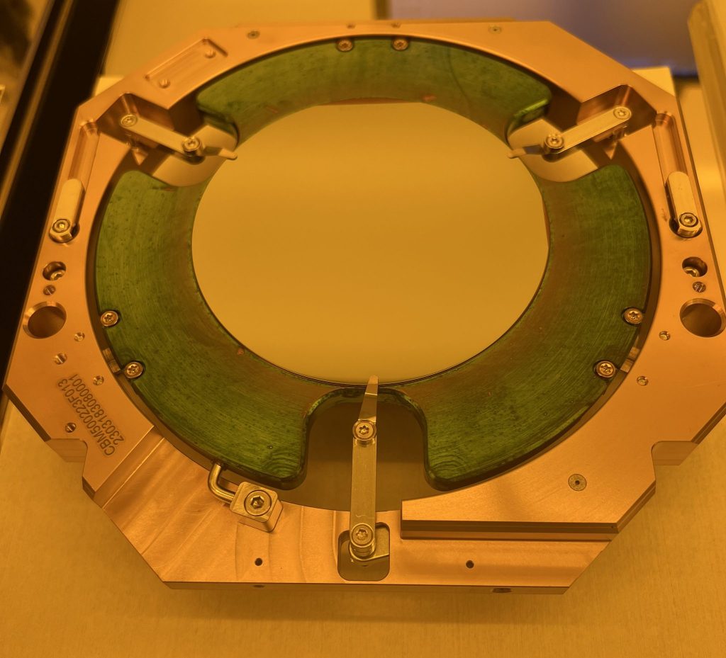
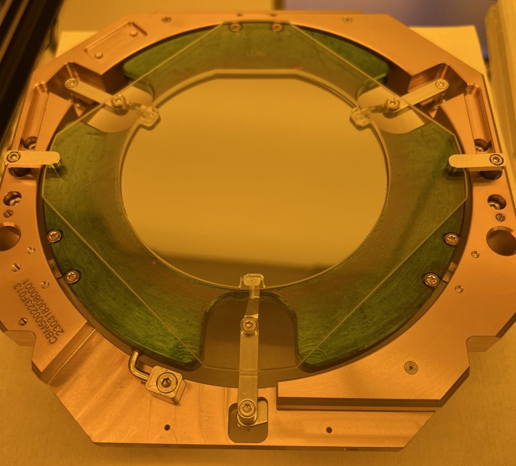
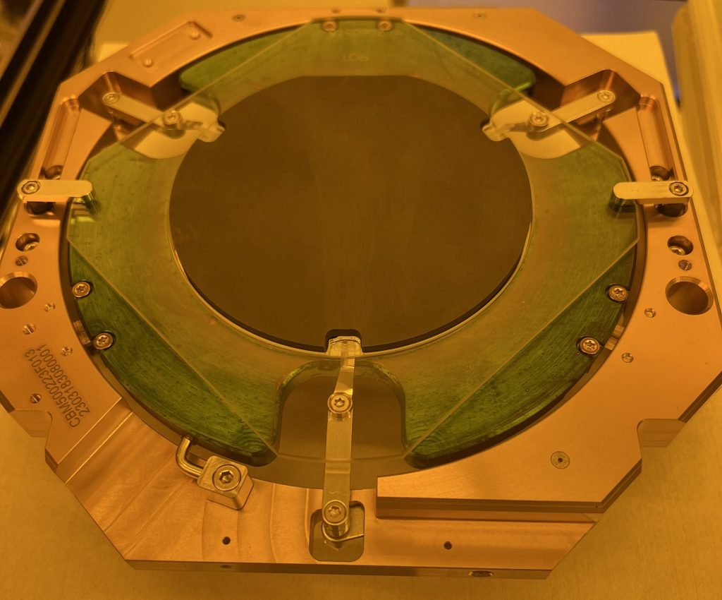
EVG 510 & 610 wafer bond chuck:
In the EVG 510 chamber, the wafers are mounted on a mechanical fixture, the “bond chuck” that features 3 x 120 deg. spacer units (flags) and 2 clamps to maintain the stack of wafers together during the whole bonding process. The bond chuck is prepared either manually or in the EVG 610 bond aligner in the case where the two wafers need a critical alignment. The steps to mount a silicon and a glass wafers on the fixture manually are shown in the gallery:
EVG 510 tool configurations:
Several parts in the bonding chamber, including the bond chuck and pressure insert, will be exchanged depending on the chosen bonding method to guarantee an optimal process stability and avoid cross-contamination between different processes.
8 sets of bond chucks and pressure inserts are available in CMI for 4 different process types, and both 4 and 6 inch wafer configurations :
- Clean bonding : Bonding of wafers with clean and dry surfaces (oxides, nitrides, silicon, glass) that “naturally” stick together due to Van der Waals chemical interactions. The stack typically requires a post-annealing step at high temperature to create covalent bonds and result in high bond strengh, but plasma surface activation (in EVG 810) coupled with DI water rinse (in EVG 301) prior to the bonding step can promote the generation of covalent bonds at low temperature.
- Anodic bonding (conductive chuck) : Bonding of silicon to borofloat 33 glass wafers or metal to glass wafers by the application of an electric field at the interface, promoting the migration of ions and the formation of a stable interface oxide.
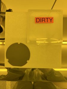
- Dirty bonding (i.e. with polymers/glue/metals) : Bonding of wafers using an intermediate material. The intermediate material can be of different type: an adhesive polymer (BCB, Su8, polyimide), a metal (thermocompression bonding, typically with Au or Al), an eutectic metal alloy (Au:Sn, Au:Si, Au:Ge,…) or a spin-on glass (glass frit, SOG).
- Infrared (IR) alignment with EVG 610 (scroll down for more details on this feature).
Users will need to request for specific configurations when booking the equipment.
The three EVG 510 tool configurations are :
|
CLEAN |
Direct (no metals) |
| ANODIC | Anodic bonding |
|
DIRTY |
Adhesive, eutectic, glass frit bonding Thermocompression bonding, direct bonding (with traces of metals) |
The change of configurations of the tool is performed by the CMi staff according to the booking table. When starting their work on the tool, users should verify that the capping quartz plate corresponds to the requested configuration (check label on the box).
EVG 610 alignment methods:
Depending on the physical properties (bulk material, transparency, surface finish) of the wafers you are trying to bond, you may choose between 3 different alignment configurations, each with specific requirements:
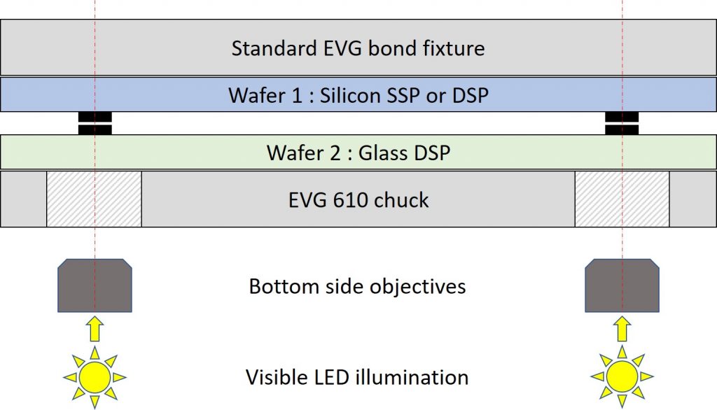
| TYPE | Wafer 1 | Wafer 2 | Illumination | Marks side (bond interface or opposite) | Marks position [um] |
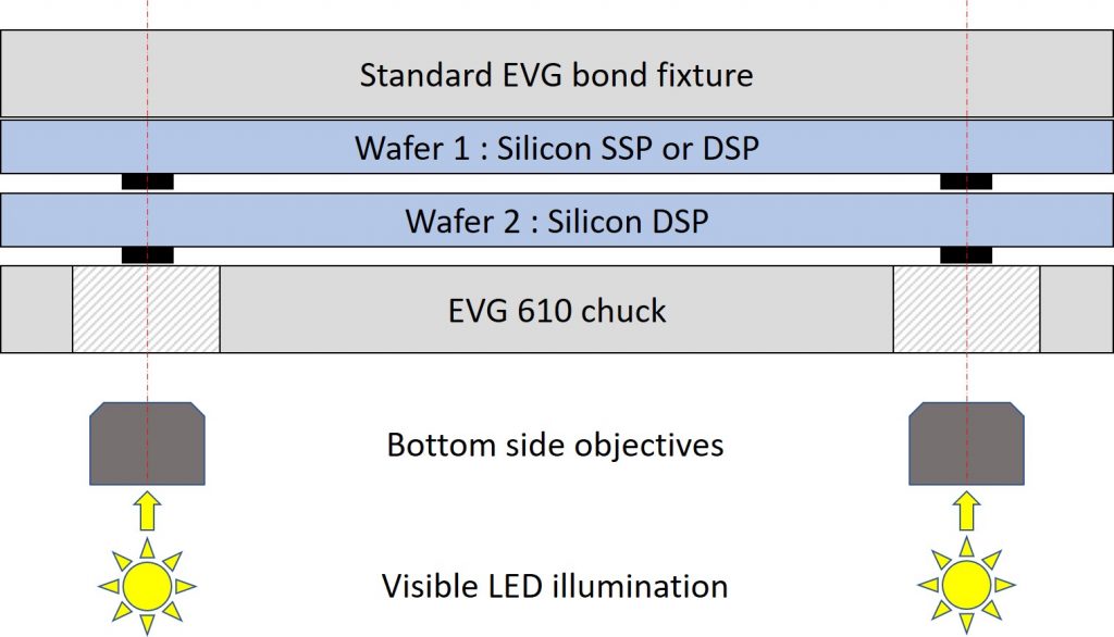
| A | Silicon SSP or DSP | Glass DSP | Visible |
Wafer 1: bond side Wafer 2: bond side |
+/- 15000 < X < +/- 45000 +/- 10000 < Y < +/- 10000 |
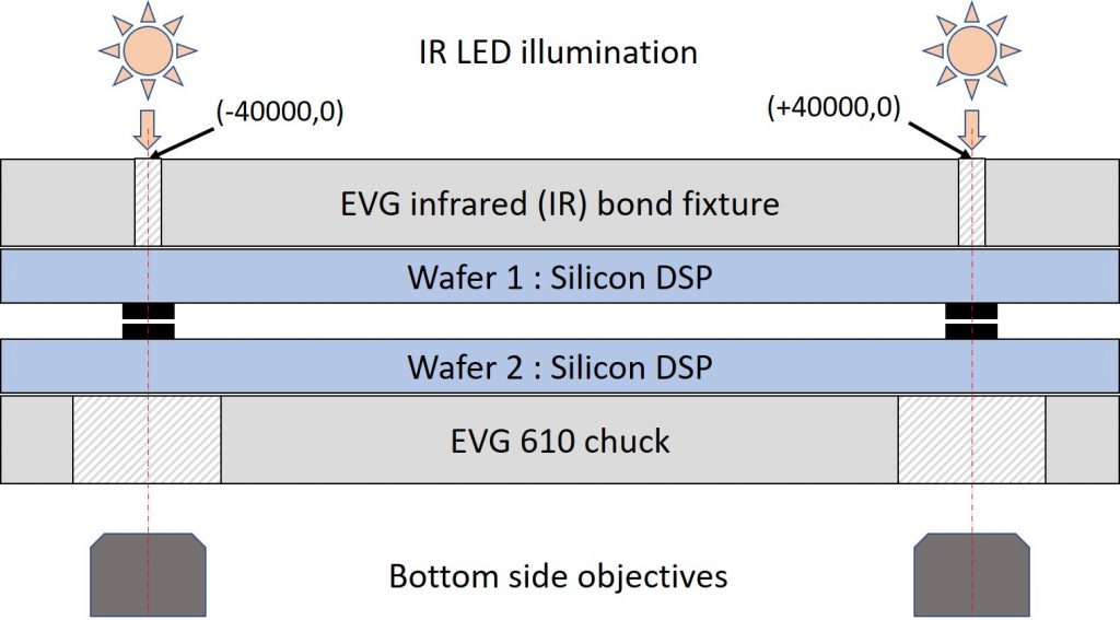
| B | Silicon DSP | Silicon DSP | Infrared (IR) |
Wafer 1: bond side Wafer 2: bond side |
X = +/- 40000 Y = 0 |
| C | Silicon SSP or DSP | Silicon DSP | Visible |
Wafer 1: bond side Wafer 2: opposite side |
+/- 15000 < X < +/- 45000 +/- 10000 < Y < +/- 10000 |
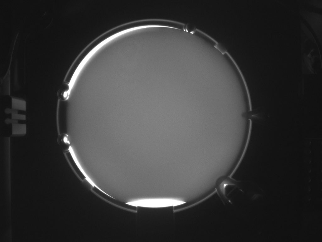
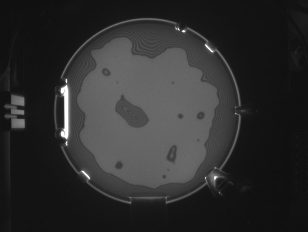
EVG 301 IR Inspection module:
An infrared (IR) illumination/inspection module is available on the EVG 301 wafer cleaner that allows inspection of the quality of the contact between two opaque wafers (Si) at the pre-bonding or a the final bonded state, and look for the presence of unbonded areas (voids).