The CMi’s SEM Crossbeam 550 is exclusively reserved for imaging dedicated to the control of processes which have been done in the CMi by the regular CMi users.
RESERVATION POLICY (starting from January 2024):
- 2 booking slots maximum per day and per person (ie. 1h).
- 6 booking slots maximum per week and per person (ie. 3h).
- Penalty charges for unused booking, late cancellations, and mismatch between booked name and operator name apply.
Saved pictures are available on STI network (EPFL local or VPN): “\\vpa-nas1.rcp.epfl.ch\cmi-images\Z15-SEM-Crossbeam“.
Offline analysis and metrology is available with ProSEM software, MountainsMap 8.2 (coupled to 3DSM Metrology), SmartStitch (room BM 1132).
AVAILABLE TRAININGS:
Basic training session is mandatory and it can be requested via the CMi website internal section. The training focuses on highligting differences between SEM Crossbeam and SEM MERLIN, being fully trained on SEM MERLIN is a prerequisit.
- Training session for aBSD detector (Annular Backscatter Detector) that provides significant utility by delivering highly contrasted imaging of samples. With its annular design, it enables visualization of composition, density, and surface topography contrasts with high sensitivity, facilitating precise analysis of samples, particularly in materials science and related fields.
- Training session for Variable Pressure Secondary Electron (VPSE) detector that serves a crucial role in imaging samples under variable pressure conditions. It allows for the observation of non-conductive specimens without the need for extensive sample preparation. By detecting secondary electrons emitted from the sample surface, the VPSE detector enables high-resolution imaging, making it invaluable for research in fields such as materials science and nanotechnology.
ProSEM is an advanced SEM metrology and automation package for monitoring of micro and nanostructures, process calibration and lithographic patterns.
System description
Overview
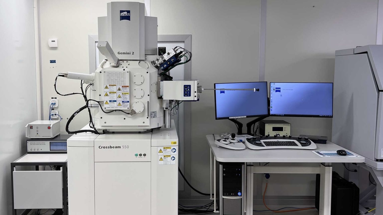
The CMi SEM Crossbeam 550 is composed of a GEMINI II column, a process chamber with a 5-axes motorized stage (X, Y, Z (M), Tilt and Rotation) and a semi-automatic airlock. The process chamber stands on a plinth entirely surrounded by protective cover panels. The system is mounted on a set of several active suspensions to compensate for vibrations. A PC equipped with two monitors allows the control of the microscopy system via a dual joystick and a dedicated control panel on the work desk.
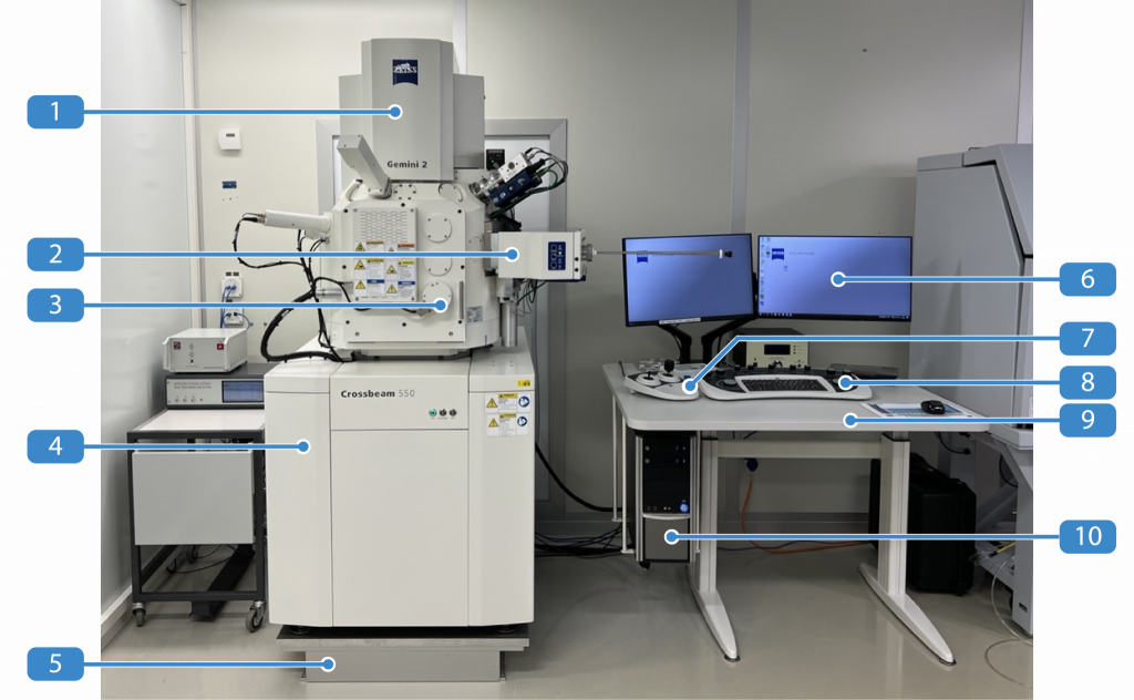
- GEMINI II electron optical column
- Airlock for fast and efficient specimen transfer and fast pumping times
- Specimen chamber with door handle
- Plinth with ON/STANDBY/OFF buttons
- Active suspension – Vibration compensation (always activated)
- Monitors
- Dual joystick
- Control Panel (Keyboard)
- Work desk
- Personal Computer (PC)
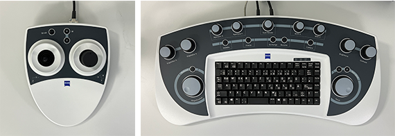
The SEM is controlled by the Zeiss SmartSEM software operated via a graphical user interface. The system is also fitted with a dual joystick for stage control and specimen navigation and with a main keyboard control panel for direct access to 14 of the most frequently used functions on the SEM.
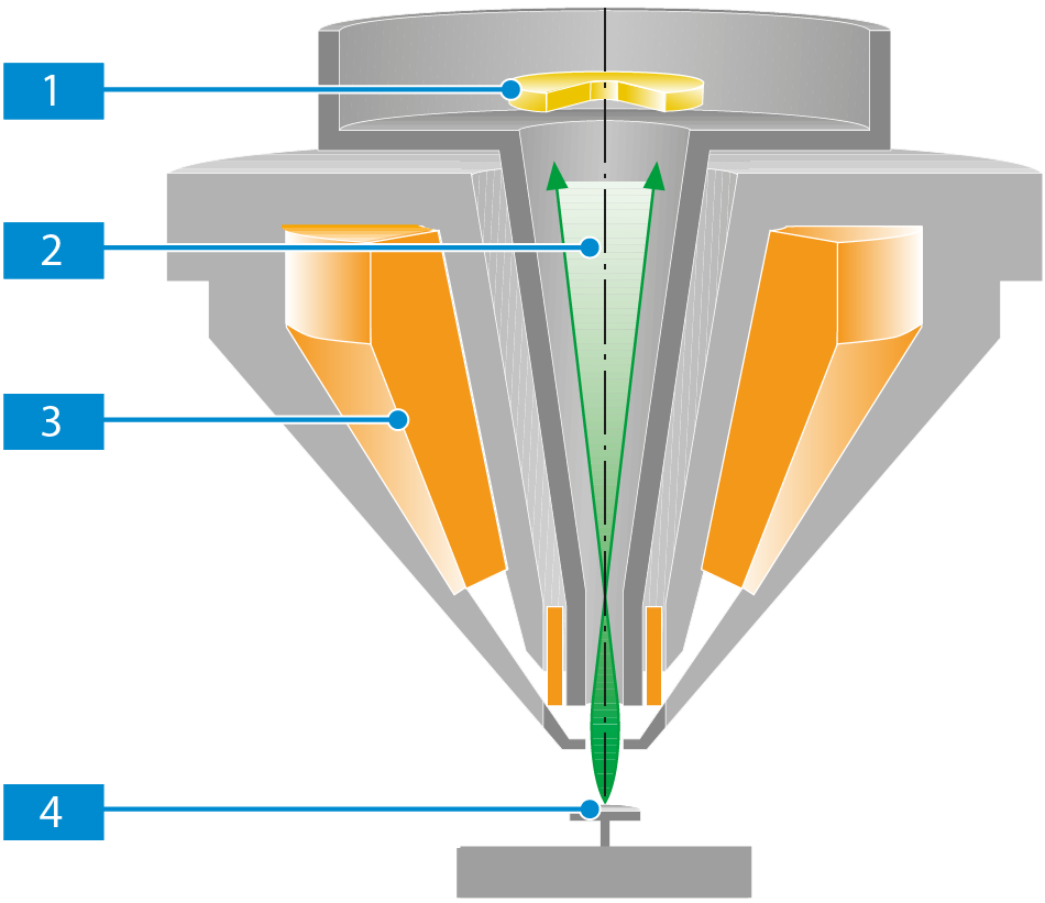
The GEMINI II column
The GEMINI II column is the part of the microscope, where electrons are emitted, accelerated, deflected, focused, and scanned. Main characteristics of the GEMINI optics are the beam booster and an objective lens that consists of a combined electrostatic/electromagnetic lens doublet.
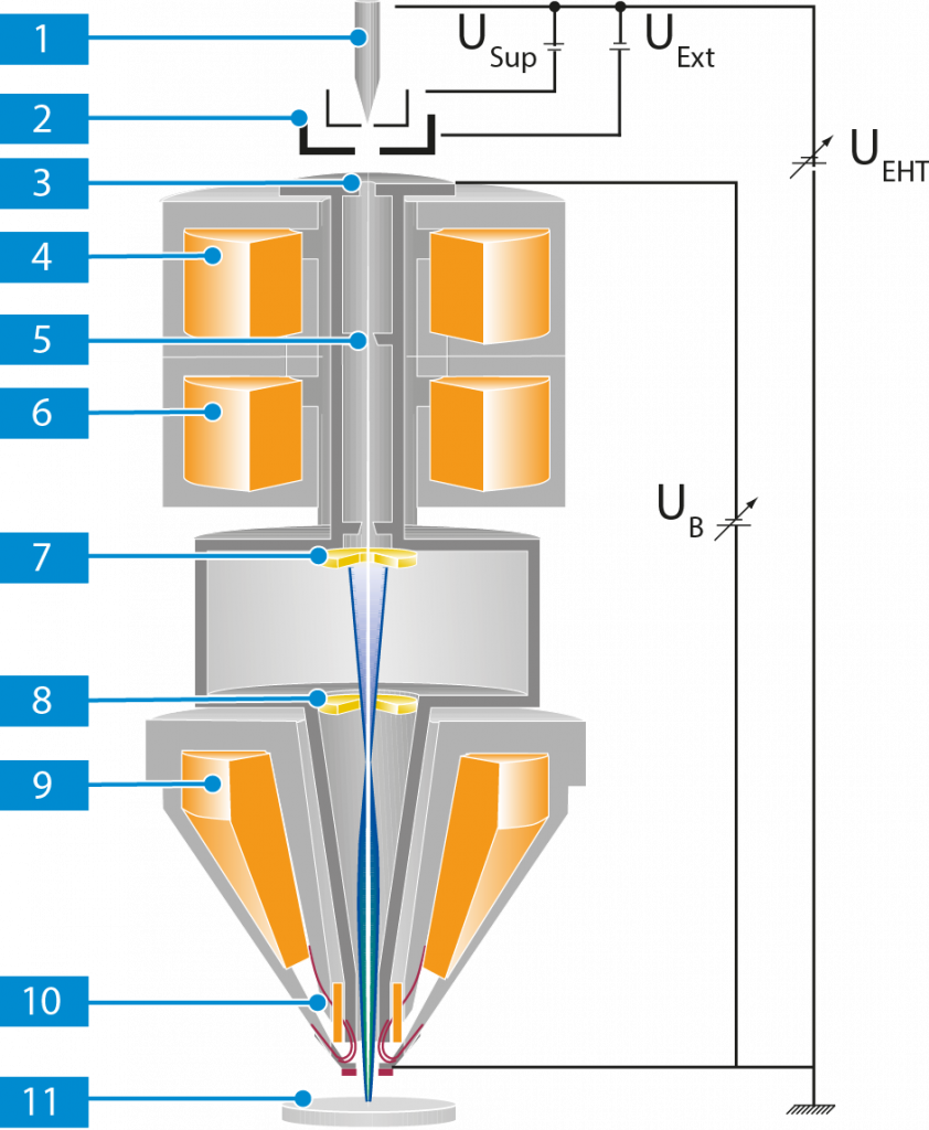
A Schottky field emitter serves as gun (1) . The filament is heated by applying the filament current. Electrons are emitted from the heated filament while an electrical field, called extractor voltage (UExt), is applied. To suppress unwanted thermionic emission from the shank of the Schottky field emitter, a suppressor voltage (USup) is applied as well.
The emitted electrons are accelerated by the acceleration voltage (UEHT). The beam booster (UB, booster voltage), which is always at a high potential if the acceleration voltage is 20 kV or less, is integrated directly after the anode. This guarantees that the energy of the electrons in the entire beam path is always much higher than the set acceleration voltage. This considerably reduces the sensitivity of the electron beam to magnetic stray fields and minimizes the beam broadening.
Detectors
Principle of Signal Detection
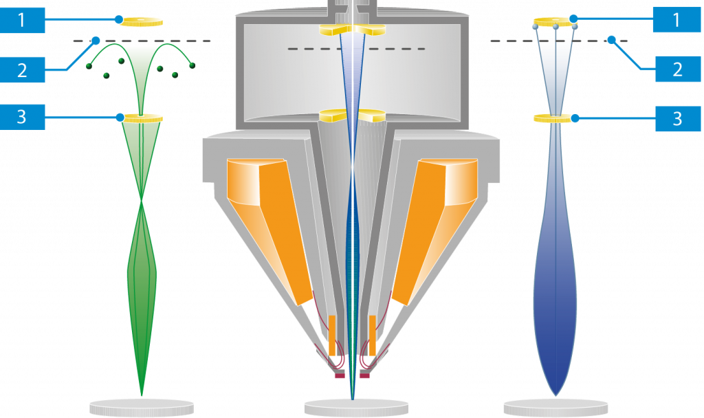
The interaction products most frequently used for the generation of images in scanning electron microscopy are secondary electrons (SEs) and backscattered electrons (BSEs).
Primary Electrons (PEs)
Primary electrons are electrons forming the scanning beam before hitting the specimen.
Secondary Electrons (SEs)
Secondary electrons are emitted from the topmost layer of the specimen.
SE1 Electrons
Electrons emitted at the point of impact between the beam and the specimen are known as SE1 type electrons. The amount of electrons emitted at the point of impact is related to the shape of the specimen.
Secondary electron detectors, such as the InLens SE detector, collect SE1 type electrons from the surface layer of the specimen and are thus ideal for displaying surface structures.
SE2 Electrons
The emergence of backscattered electrons from the specimen excites further emission of secondary electrons. These are known as SE2 type electrons.
Detectors that collect SE2 type electrons are especially suitable where the working distance is large. Surface detail as the effect of “lateral illumination” emphasizes the topography of the specimen.
Backscattered Electrons (BSEs)
Backscattered electrons (BSEs) emerge from below the surface of the specimen (up to an order of μm). The number of electrons emitted at the point of impact is highly dependent on the meanatomic number of the specimen material. This means that a BSE image provides depth information and atomic number contrast.
BSE detectors are used to display the materials contrast because the backscatter coefficient is dependent on the mean atomic number of the material under investigation.
Detector Overview – Available detectors
The beam scans the specimen and initiates particles to be emitted. A detector collects the emission and produces an electric signal with an amplitude proportional to the number of particles at any given time.
| Standard detectors | Detected Signals | Typical Application |
|---|---|---|
| InLens SE Detector | SE1 | Surface structure |
| SE Detector | SE2 | Topography |
| Optional Detectors | Detected Signals | Typical Application |
|---|---|---|
| EsB Detector | SE1 BSE | Surface structure Material contrast |
| aBSD Detector | BSE | Angular resolved BSE imaging Compositional contrast |
| VPSE Detector | Light Photons | Non-conductive samples |
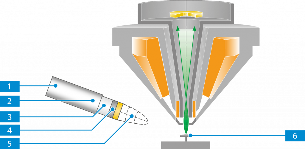
InLens SE Detector
The InLens SE detector is a high-efficiency detector for high resolution SE imaging and detects secondary electrons directly in the beam path. The detection efficiency of this detector results from its geometric position in the beam path and from the combination with the electrostatic/electromagnetic lens.
The primary electrons are accelerated by the acceleration voltage at the anode and, up to an acceleration voltage of 20 kV, by an additional beam booster voltage of 8 kV at the liner tube. To ensure that the electrons reach the specimen surface 4 with the energy set as acceleration voltage, an opposing electrostatic field of the same magnitude as the beam booster voltage (8 kV) is generated at the end of the objective lens by the electrostatic lens. This electrostatic field acts as acceleration field for the SEs generated on the specimen surface.
At the InLens SE detector, the electrons hit a scintillator. This generates a flash of light that is led out of the beam path and onto a photomultiplier by means of a lightguide. The photomultiplier converts the light information into an electronic signal, which can be displayed on the monitor.
The efficiency of the InLens SE detector is mainly determined by the electric field of the electrostatic lens, which decreases exponentially with the distance.
Thus, the working distance (WD) is one of the most important factors affecting the signal-to-noise ratio of the InLens SE detector.
As the tilt angle of the specimen surface affects the emission angle of the electrons, you should avoid strong specimen tilting.
SE Detector
The SE detector is an Everhart-Thornley type detector. It detects SEs as well as BSEs. The SE detector is attached to the options ports plate.
Electrons moving to the detector are attracted/repelled by the collector grid and directed to the scintillator. The electrons gain energy from the scintillator and thus are able to interact with a phosphor layer, which generates photons (light). The light travels up a light pipe to a photomultiplier. The photomultiplier multiplies the flashes of light and outputs a signal that can be used for imaging.
The collector voltage can be varied in the range between −250 V and +400 V.
A positive collector voltage generates an electrical field in front of the detector, thus directing the low energy SEs towards the scintillator.
EsB Detector
The Energy-selective Backscattered (EsB) detector enables both SE and BSE detection. It can be used for high contrast topography or for compositional contrast examinations.
The SEs and BSEs generated at the impact point of the primary electron beam are intercepted by the low electrical field of the column. These electrons are accelerated by the field of the electrostatic
lens.
The annular shaped in-column detector is located above the InLens SE detector.
aBSD detector
The aBSD detector is a pneumatically retractable annular BackScattered electron Detector. It is used for high efficiency and angle selective material characterization even at low-kV applications.
It has five separate diode segments, one inner concentric ring and four outer quadrants. The inner segment provide mostly material contrast whereas the four outer quadrants provide more topographical
contrast.
Chamber CCD Cameras
The microscope contains a CCD camera (charge-coupled device camera) inside the specimen chamber. It is referred to as the chamber CCD camera or chamberscope. It allows you to monitor the position of the specimen stage and particularly the distance between the objective lens and
the specimen holder.
The chamber CCD camera is located at the backside of the specimen chamber. A second CCD camera is installed on the left-hand side of the specimen chamber.


Use the chamber CCD camera to monitor the position of the specimen holder during stage movements. Pay particular attention to the distance between the objective lens and the top of the specimen. This applies to vertical movements, but also to horizontal movements, because a thick specimen may collide with the objective lens from the side.
The image of the chamber CCD camera can be adjusted by the user:
- Brightness, contrast, and CCD illumination can be optimized to improve the image.
- Certain display details can be chosen by zooming in and shifting. This can be achieved by turning the Magnification and Shift X or Shift Y knobs on the control panel, respectively.
Specimen Stage & Holders
Specimen Stage
The motorized eucentric specimen stage is used to navigate the specimen inside the specimen chamber.
The specimen stage is mounted on the chamber door. If the chamber door is closed, the specimen stage is inside of the specimen chamber.
When moving a tilted stage in X/Y direction, no displacement (moving out of focus) occurs. When a pre-tilted specimen holder is used, X/Y movements require an adjustment of the Z position to stay in focus.
The stage can be operated using the Dual Joystick or using the SmartSEM software.
| Axis | Description | Movement |
|---|---|---|
| X | X-axis | Movement towards or away from the chamber door (horizontal movement in the image) |
| Y | Y-axis | Movement |
| Z | Height | Vertical movement (movement towards or away from the focal plane of the image) |
| M | Height | Movement of the specimen surface into the tilt axis at various working distances |
| R | Stage rotation parallel to the X-Y plane | |
| T | Stage tilt about an axis parallel to the X axis |
The stage is eucentric, which means that the tilt axis intersects the beam axis. The specimen surface is located in the eucentric point, where the tilt axis meets the beam axis. This guarantees that the focus and the point of interest are maintained when the specimen is tilted at a certain working distance.
Holders
Five different holders are available:
- Carousel 9x10mm, multi-pin holder (mono samples, eg. small chips),
- Wafer Section (cleaved samples),
- 4 Inch Wafer,
- 6 Inch Wafer,
- 6 Inch Mask.
Each sample holder allows the imaging of a particular type of sample. It is strongly not recommended to use them for anything other than their intended purpose, as this could result in significant material damage to the imaging chamber.
A complete set of accessories allows to mount cleanly any kind of specimen on the different specimen holders available (screwdriver, tweezers, carbon sticker, blade for removing stickers, pin-holder, Cu tape etc.).
Basic operations
Login/logout on CAE
First, the tool needs to be activated by logging onto CMi Zone 15 computer with personal access rights through Control Access Equipment (CAE) software. If you forget to login, you will not be able to use the SEM computer.
Windows session
On the SEM local computer, the Windows operating system is always open and running through standard CMi session. Otherwise, you can find username and password on bottom of the screen.
SmartSEM session
The SmartSEM Program Suite comprises the EM server, which implements the internal communication between control software and microscope hardware, plus several programs and utilities.
The main purpose of the SmartSEM Program Suite is to access all necessary microscopy parameters and software features to capture SEM data and optimize image acquisition.
Access: Windows start menu > SmartSEM
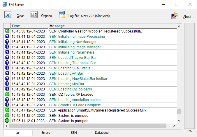
Note: If the EM Sever was accidentaly closed by the last User, Starting the Zeiss SmartSEM software will first reload the EM server and recover software/hardware communication.
SmartSEM User Interface
The user should refer to the MERLIN instruction manual for routine operations as well as for an explanation of the features available through the various buttons on the system interface.
The SmartSEM software graphical user interface (GUI) allows you to monitor and operate most of the active components of the microscope.
Starting SmartSEM
1. Start the SmartSEM user interface via the ZEISS SmartSEM icon on the desktop.
![]()
Alternatively, select Windows start menu > SmartSEM > SmartSEM User Interface.
→ The EM Server opens while loading various drivers. The EM Server implements the internal communication between software and hardware of the microscope.
→ The EM Server Log On dialog is displayed.
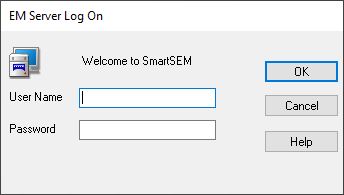
2. Enter the user name and password.
3. Click OK.
→ The SmartSEM user interface opens and is ready to operate the microscope.
The following screenshot indicates the main elements of the SmartSEM user interface:
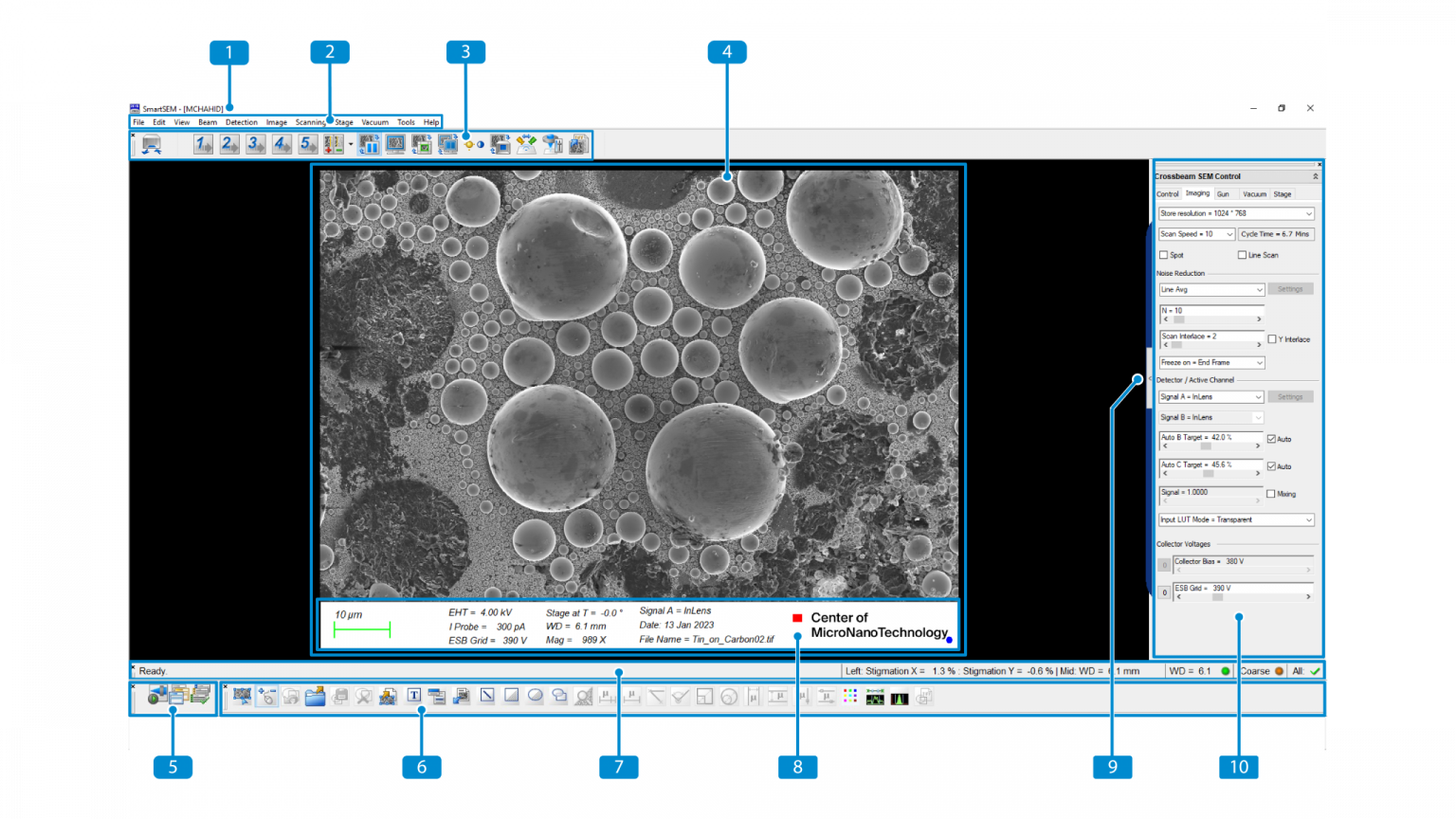
Screen layout of the user interface
(1) Title Bar – Displays the name of the user interface and the
logged-on user.
(2) Menu Bar – Enables you to access to SmartSEM features via sub-menus.
(3) Toolbar – Provides quick access to SmartSEM tools.
(4) Image Area with Data Zone – Displays image information and acquisition parameters from the microscope.
(5) Mini Bar – Provides quick access to recently used dialogs and to the recipe management.
(6) Annotation Bar – Enables you to add information to the SEM image and provides several measurement functions.
(7) Status Bar – Displays the current machine state and contains the SEM Control Buttons.
(8) Data Zone – Displays image information and acquisition parameters from the microscope.
(9) Panel Configuration Bar – Enables you to choose the panels to be placed in the Docking Panel.
(10) Docking Panel – Enables you to arrange frequently used SmartSEM panels for convenient access.
The main difference with the MERLIN SmartSEM interface is located within the Docking Panel (10) (cf. below).
This section describes basic procedures to obtain an image using the SE detector. To simplify the procedure, the description uses the Crossbeam SEM Control panel and status bar functions in the SmartSEM software.
The main difference with the MERLIN SmartSEM interface is located within the Docking Panel (10) (cf. above).
The use of the basic functions of this microscope is identical to that of the SEM MERLIN. The specificities are developed during the mandatory training for users who have already been trained and have a fairly advanced practice on the SEM MERLIN.