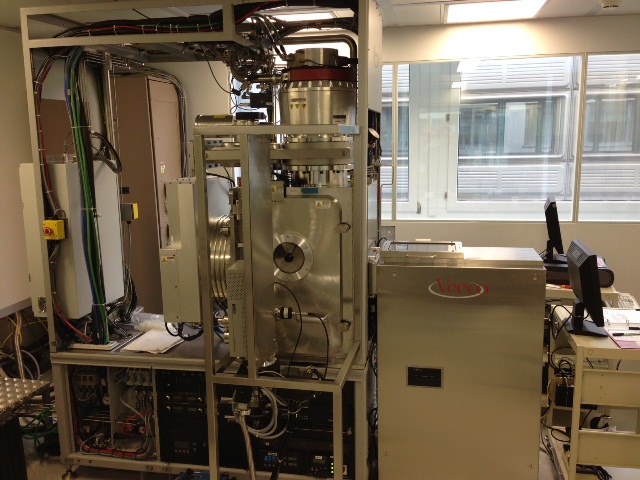
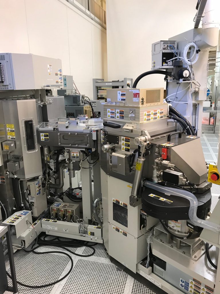
– 100mm wafers (max 4mm thick) – Argon ions 350mm broad-beam – Large range energy capability (50V to 800V) – High uniformity and high collimation – Pure physical sputtering of any material – Low temperature substrate fixture (<90°C) – Secondary Ions Mass Spectroscopy – Location: Zone 11
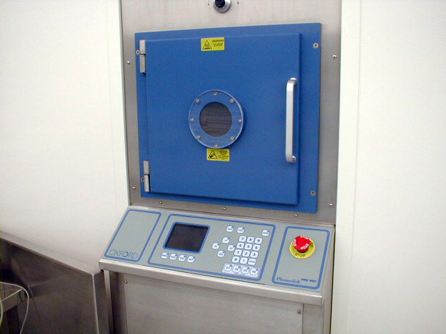
Samples must NOT have presence of any metallics, or traces of metallics (real or suspicion), even buried. – ICP plasma etcher 100mm wafers – Fluorine chemistry – Electrostatic clamping – Microelectronic compatible equipment – SiO2 and Si3N4 thin films etching – Optical Emission Spectroscopy (EOS) end-point-detection – Laser reflectometry/interferometry end-point-detection – Location: Zone 2
Samples must NOT have presence of any metallics, or traces of metallics (real or suspicion), even buried. – DRM (Dipole Ring Magnet) – 100mm – RIE with magnetic field assistance – Fluorine chemistry – Electrostatic clamping – Microelectronic compatible equipment – SiO2 and Si3N4 thin films etching – Optical Emission Spectroscopy (EOS) end-point-detection – Location: Zone 2
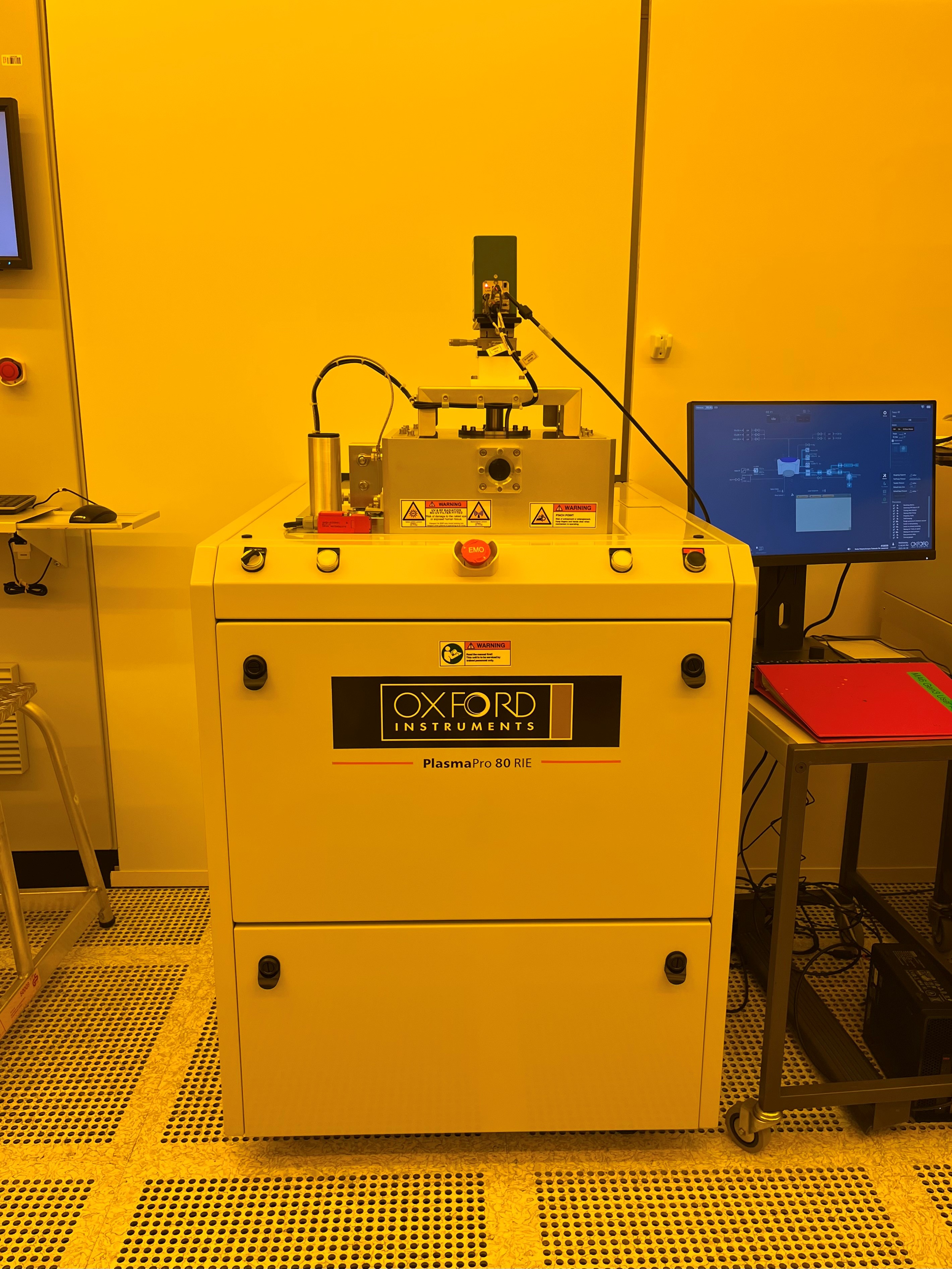
– RIE plasma etcher – CHF3, SF6, O2, Ar – Max 300W @ 13.56MHz – Open-load system (no load lock) – Chips to wafer up to 200mm – hBN, SiGe, Graphite and Graphene soft etching – Location: Zone 3
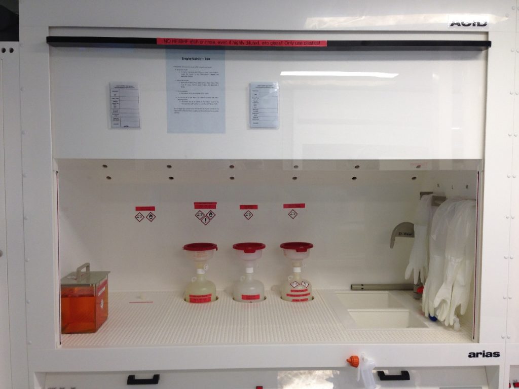
– 8 inches wafers to piece parts – HF chemistry – SiO2 etch – Controllable etch rate (nm/min to um/min) – Dry process without sticking issues – Location: Zone 2
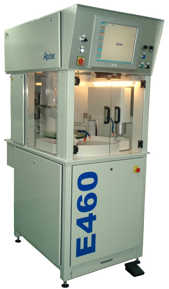
– Silicon, III/V materials and glass types grinding – Single wafers, stacked wafers and chips (from a few mm2 to full 8″ wafers) – Frame mounting on UV-tape – Disco DCS1440 atomizing cleaning – Roughness < 100nm, TTV ~ 1micron – Location: Zone 22
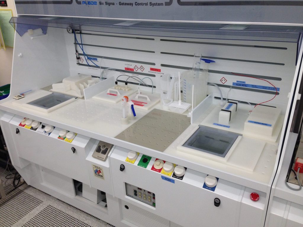
– 100, 150 mm wafers and piece parts – 100 mm chuck to protect wafer back side – KOH chemistry 40%/60°C – Silicon anisotropic etch – Location: Zone 18/19