When creating a pattern on a wafer with photolithography, you must describe or digitize the pattern using geometric shapes to identify areas where UV light will expose the photoresist and areas where it will not. This step is necessary for fabricating a Cr blank mask or exposing the photoresist with a UV laser (direct laser writing).
Table of content
- Layout Formats
- Layout Editors
- Layout Design Rules
- Alignment marks
- Vernier
- CMi Layout Templates
Layout Formats
To create a complete 2D layout, patterns can be drawn using CAD software, generated with mathematics software like Matlab or Octave, or coded with Python/Ruby scripts. Various layout file formats exist, some proprietary, some public, and some standard. Regardless of the CAD software used, the design should be exported to formats compatible with equipments used at CMi, such as (in order of recommendation):
(Graphic Database System for Information Interchange)
The GDS file format is an industry standard and the recommended file format to flawlessly convert your design to the internal language of the HIMT direct laser writing equipment. General information about the GDS format are available here.
(Drawing Exchange Format)
The DXF file format as been developped by Autodesk to enable data exchange between AutoCAD and related softwares. With many limitations and restrictions, DXF files may be accepted and converted correctly by the HIMT conversion tool. General information about the DXF format are available here.
(Caltech Intermediate Format)
The CIF file format is a concise and human readable text based description of the layout. In general, the CIF format is converted without issues but some proprietary text statements introduced in specific layout editors (such a Clewin) may not be interpretated correctly by the HIMT conversion tool. General information about the CIF format are available here.
Layout Editors
Below is a list of the softwares that are recommended by the CMi to create your designs in the accepted file formats.
by Matthias Köfferlein, Klayout.de
- Free software
- Download links available on the Klayout website
- Installed on all CMi computers (machine and zones)
It is possible to use python to create your design. The following libraries have been used succesfully by CMi staff or users :
by Mentor (Siemens), website
- Distributed to EPFL through EUROPRACTICE membership
- Utilization is strictly reserved to EPFL employees and students. No utilization of the tool can be done for commercial purpose.
- Network license pool
- Contact the photolithography staff for installation files & licensing instructions.
by Bay Technology
- License for CMi users
- Contact the photolithography staff for installation files & licensing instructions.
- Installed on CMi open office BM 1.132 computers
| Software | Description | License/Installation |
| Clewin (v4) |
by WieWeb software, layout editor |
|
| Solidworks | by Dassault Systems, mechanical drawing software |
|
| by Ulf Griesmann, Matlab/Octave GDS import/modify module |
|
|
| by Lucas Heitzmann, C++ & Python GDS/OASIS import/modify module |
|
|
| LayoutEditor | by Juspertor GmbH, layout editor |
|
| Glade | by Peardrop Design Systems, layout editor |
|
| Virtuoso Layout Suite | by Cadence, professional layout suite |
|
| Expert | by Silvaco, professional layout suite |
|
Layout Design Rules
The user is free to create whatever design he wants, but to be exposed in a laser writer, it must only contain polygons (= closed polylines). One should not use path and increase its width to create channels, waveguides, etc.. Curves and circles can only be created by an approximation with segments.
On top of these limitations, the CMi has a few recommendations :
Leave 3mm free on the outer edge of the wafer
Any critical device placed in this area is much more likely to have different characteristics than if it was in the center due to process limitations or manipulation with mechanical tweezers.
Alignment marks
Every machine has a different field of view and working principle to use alignment marks. Below are the recommendations for each machine.
The coordinates of alignment marks should not have a precision that is below 0.1um. There is more chance that a rounding error occurs than improving the alignment quality. Also it is advised to place the alignment marks at round coordinates.
Make sure to also include visual directional guidelines (arrows, grids,…), as part of your layout, to easily locate your marks on the wafer and/or mask. Without it, since the field of view of the alignment systems are usually quite small you may lose a considerable ammount of time trying to locate a tiny cross in the middle of nothing else.
Field of view :
- Rotating camera : 375um x 500um
- Objective lens 10x : 415um x 550um
- Objective lens 5x : 825um x 1100um
The CMi recommend :
- Layer 1 – Cross (thickness : 6um / length : 180um)
- Layer 2 – Design to align around the cross

It is advised to leave a small gap between the two parts of the marks (e.g. 1um) for ease of alignment.
The CMi also strongly recommends to create an open window around the Layer 2 mark in order to better see the wafer underneath.
All these recommendations are applied in the CMi template MASK.
Field of view :
- MLA1
- LowRes : 645um x 430um
- HighRes : 190um x 125um
- MLA2
- LowRes : 490um x 390um
- HighRes : 220um x 150um
The CMi recommends :
- Cross (thickness : 20um / length : 190-300um)
- Minimum of 2 crosses for offset correction
- Minimum of 4 crosses for expansion and shear correction
- No more than 2 marks should share similar X or Y coordinates
- Examples of coordinates for 4in wafer :
(±40000um ; ± 40000um)
All layers can be aligned on the same crosses as long as they stay visible.
For backside alignment, the machines are not able to see everywhere under the wafer. Areas where marks can be found are in the CMi template LASER.
All these recommendations are applied in the CMi template LASER.
Field of view and cross dimensions :
- 20mm Write Head
- Macro : 895um x 740um
- Micro: 460um x 345um
- Cross (thickness : 65um / length : 650um)
- 10mm Write Head
- Macro : 545um x 410um
- Micro: 220um x 165um
- Cross (thickness : 30um / length : 300um)
- 4mm Write Head
- Macro : 205um x 155um
- Micro: 85um x 65um
- Cross (thickness : 12um / length : 120um)
The CMi recommends :
- Minimum of 2 crosses for offset correction
- Minimum of 4 crosses for expansion and shear correction
- No more than 2 marks should share similar X or Y coordinates
- Examples of coordinates for 4in wafer :
(±40000um ; ± 40000um)
All layers can be aligned on the same crosses as long as they stay visible.
Vernier scale for offset measurement
The CMi strongly recommends to implement Vernier scales in all your designs to precisely measure the alignement offset from one layer to another. In all CMi templates, Vernier scales are implemented directly around the marks.
How to use Vernier scales :
In your design, a Vernier scale must be separated between the two layers you want to check the alignment with regard to each other. To check the alignment in the X direction, here is how it could look like :
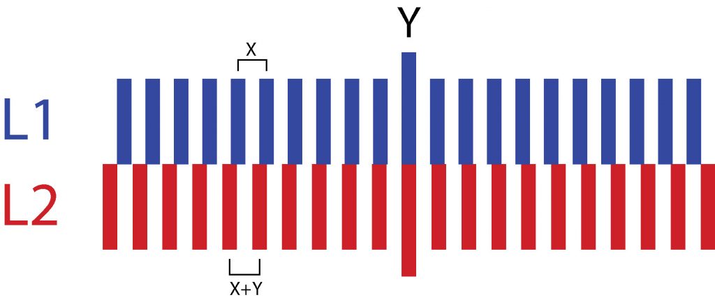
On L1 there is a scale with a constant pitch X. On L2, we also have a scale with the same center, but the pitch is now X+Y. Y being the minimum offset we will be able to detect.
In practice, when you expose L2 on L1, if the Vernier looks exactly like the one in your design, it means there is no offset. However, in practice, there is more chance the L2 scale will not be centered anymore, as presented in the figure below.
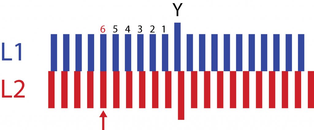
In this case, to determine the offset, you have to find which bars of both scales perfectly align on top of each other. In our case, it is the sixth one on the left, and the offset is therefore equal to 6*Y.
CMi Layout Templates
You will find below basic CAD layout templates to use on CMi exposure equipments:
LASER template
The LASER template is available for users that mainly operates the CMi direct laser writers (MLA 150, VPG 200) for the photolithography patterning steps. Description of the layers used in the template:
| GDS # |
Layer function
|
Notes |
| 10 |
Wafer frame
|
This layer shows the last 3mm edge area from a 100mm SEMI wafer where it is not recommended to place devices. All critical cells/layers should be drawn in the white inner area. This layer is normally removed from the layout. |
| 20 |
Alignment marks
|
This layer shows a set of 4 cross alignment marks that can be exposed during the first lithography step and used during the alignment sequence of the following exposed layers. Marks coordinates, in [um], are at (+/- 40000, 0) and (0,+/-40000). An alternate set of square marks are located at (+/- 39000, 0) and (0,+/-39000). For topside alignment (TSA), the marks can be moved, to adapt to the device, to any position on the wafer. For backside alignment (BSA – MLA 150 only), the marks should stay along the x- or y-axis in the stage open window areas (see layer 60). |
| 21 |
Vernier patterns
|
This layer shows an example of vernier patterns, matching with the alignment marks layout, that can be exposed at the second lithography step to measure the critical alignment with the first exposure. |
| 40 |
Dicing marks
|
This matrix of crosses show an example guideline set for dicing the wafer into dies. The layer should be kept only if dicing will occur; the step size can be adjusted to adapt to the device dimensions. |
| 60 |
MLA 150 BSA areas, vacuum lanes.
|
This layer shows the MLA 150 vacuum lanes and the position of the 4 open stage windows where BSA alignment marks should be located to be visible to the backside objectives. |
MASK template
The MASK template is available for users that operates the CMi mask-aligners (MA6 Gen3, MJB4, EVG 610) for the photolithography patterning steps. Description of the layers used in the template:
| GDS # |
Layer function
|
Notes |
| 10 |
Wafer frame
|
This layer shows the last 3mm edge area from a 100mm SEMI wafer where it is not recommended to place devices. All critical cells/layers should be drawn in the white inner area. This layer is normally removed from the layout. |
| 21 |
First MASK Alignment marks
|
This layer shows two sets of alignment marks (left and right) that should be included in the mask used for the first lithography step. On each side, 3 marks are included for the exposure with 3 additional masks. Marks are located at (+/- 42000, 0) for mask N°2, (+/-41600, 0) for mask N°3, and (+/-41200, 0) for mask N°4. For topside alignment (TSA), the marks can be moved to any position on the x-axis. For backside alignment (BSA – MLA 150 only), the marks should stay within the chuck open windows (see layer 61). |
|
22 or 24 |
MASK N°2
Alignment marks
|
These layers (22 or 24) show the alignment marks layout that should be included on the mask N°2 and that will match with the first mask exposure at the (+/- 42000, 0) position. Layer 22 is used if your mask if fabricated in CLEAR mode. Layer 24 is used if your mask is fabricated in DARK mode. An additional set of alignment marks is printed together for critical alignment between MASK N°2 and MASK N°3. |
| 23 or 25 |
MASK N°3
Alignment marks
|
These layers (23 or 25) show the alignment marks layout that should be included on the mask N°3 and that will match with the first mask exposure at the (+/- 41600, 0) position. Layer 23 is used if your mask if fabricated in CLEAR mode. Layer 25 is used if your mask is fabricated in DARK mode. An additional set of alignment marks is printed together for critical alignment between MASK N°3 and MASK N°4. |
| 30 |
MASK frame
|
This layer shows the layout of the mask frame that can be exposed when fabricating a 5″ mask to be used with 100mm wafers. This layout includes the frame, the mask details and an open window for precise alignment of the wafer flat in first MASK exposure mode. This layer should be exposed in CLEAR mode. |
| 41 |
Dicing marks
|
This matrix of crosses show an example guideline set for dicing the wafer into dies. The layer should be kept only if dicing will occur; the step size can be adjusted to adapt to the device dimensions. |
| 61 |
MA6 Gen3 BSA areas
|
This layer shows the position of the two open windows in the chuck of the MA6 Gen3 mask-aligner where BSA alignment marks should be located to be visible to the backside objectives. |
RESOLUTION template
The RESOLUTION template is available for users that want to include a small generic pattern in their layout for the evaluation of the photolithography resolution limits or to perform dose/focus optimizations using the built-in “series” option on the CMi laser writer (MLA 150, VPG 200).
| GDS # |
Layer function
|
Notes |
| 50 |
Resolution Tests
|
This layer contains 4 test patterns which are adapted to the evaluation of resolution limits at different crititical dimensions (CD = 600nm, 1um, 2um, or 5um). You should use only one of these patterns based on your combination of resist thickness and exposure equipment/configurations. Please contact the photolithography staff for advice on how to properly use these layouts for dose/focus series optimizations. |
MIX & MATCH template
The MIX & MATCH template is available for users that wants to fabricate a “ZERO LAYER” wafer, that contains all the necessary marks to align and expose on CMI’s exposure tools (direct-laser writers, mask-aligners, DUV stepper, EBEAM litography tool). The exposition of a “ZERO LAYER” wafer can only be done on an exposure equipment with a reliable edge detection procedure (VPG200, ASML PAS 5500/350C) to guarantee the accuracy of the layout position. The layout should be adjusted to the user dimensional requirements and approved by the CMi staff. Description of the layers used in the template:
| GDS # |
Layer function
|
Notes |
| 10 |
Wafer frame
|
This layer shows the last 3mm edge area from a 100mm SEMI wafer where it is not recommended to place devices. All critical cells/layers should be drawn in the white inner area. This layer is normally removed from the layout. |
| 11 |
Stepper exposure fields
|
This layer shows the typical 9 x 9 layout of the maximal-sized fields (2.2cm*2.2cm) that can be exposed with the ASML DUV stepper. The overall layout is centered at (0;0). A 100um dicing lane separates each field. |
|
20 |
LASER
alignment marks
|
Standard cross-shaped marks that can be used for the alignment/overlay procedure on CMi laser-writers (MLA 150, VPG 200). Marks coordinates, in [um], are at (+/- 40000, 0) and (0,+/-40000). Mark positions should be adjusted to the user device layout constraints. |
| 21 |
MASK
alignment marks
|
Two sets of alignment marks (left and right) that can be used to expose with mask-aligners. 3 marks are included on each side for the exposure with 3 additional masks. Marks are located at (+/- 42000, 0), (+/-41600, 0), and (+/-41200, 0). Mark positions should be adjusted to the user device layout constraints. |
| 27 |
EBEAM
alignment marks
|
This layer contains the layout of both pre-alignment and fine, global alignment marks for the alignment/overlay procedure on CMI’s EBEAM exposure tool, Raith EBPG 5000+. Since the alignment procedure with the EBEAM tools actually exposes and potentially damages the marks, several of them are available. A first set of four pre-alignment (PAM) marks are located at (-38000, -19000), (-35000, -19000), (-38000, -22000), and (-35000, -22000). A second set of four pre-alignment (PAM) marks are located at (-19000, -35000), (-19000, -38000), (-22000, -38000), and (-22000, -35000). The EBEAM global alignment mark is a single 20um * 20um square (arranged in sets of 9 distant by 200um), positionned at five different wafer locations. The detection is done at the five positions, detecting one square only for accurate wafer overlay/alignment. Positions of the square sets are (-33300, -33300), (-33300, -11100), (-33300, +33300), (-11100, -33300), and (+33300, -33300). Mark positions should be adjusted to the user device layout constraints. |
| 28 |
DUV STEPPER alignment marks
|
The “PM” alignment mark consists in 2 sets of vertical and horizontal 8um or 8.8um line & space gratings. They can be used both for the optical pre-alignment and for the trough-the-lens (TTL) alignment procedure of the ASML PAS 5500/350C DUV stepper. The marks coordinates, in [um], are at (+/-39000, 0) and (0,+/-39000). Mark positions should be adjusted to the user device layout constraints but are restricted to certain area of the wafer if the optical pre-alignment is required. |
| 41 |
Dicing marks
|
This layout is an example of dotted patterns that can be used in the dicing lane to help with the alignment of the dicing blades. |