Restrictions and Precautions
! Wafers that were once processed in SPTS APS etcher are not allowed in TEL Unity etcher !
If any doubts, please get in touch with etching staff BEFORE proceeding.
1. Maximum allowed booking per person between 9am and 5pm is 2 hours. It is still possible to get 4 consecutive hours from 7am to 11am or from 3pm to 7pm.
2. Reservation names must correspond to operators.
Contents
I. Introduction
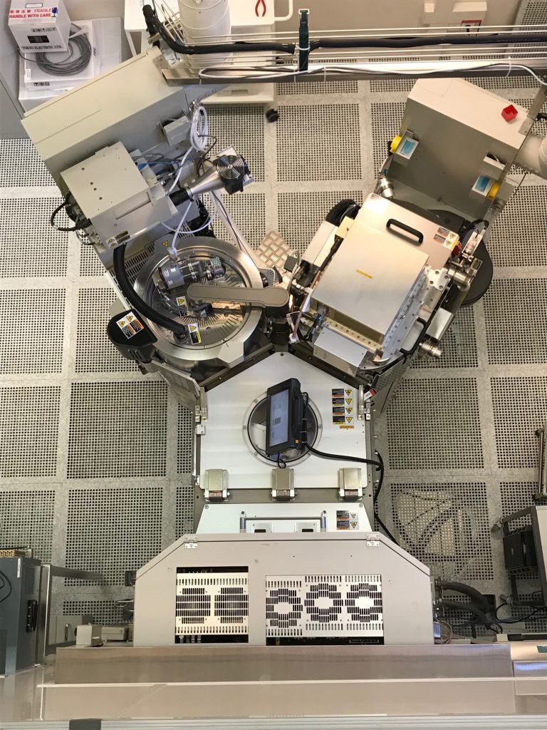
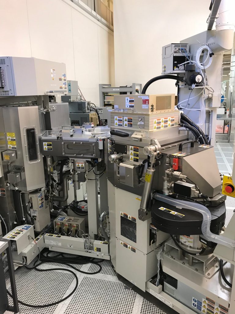
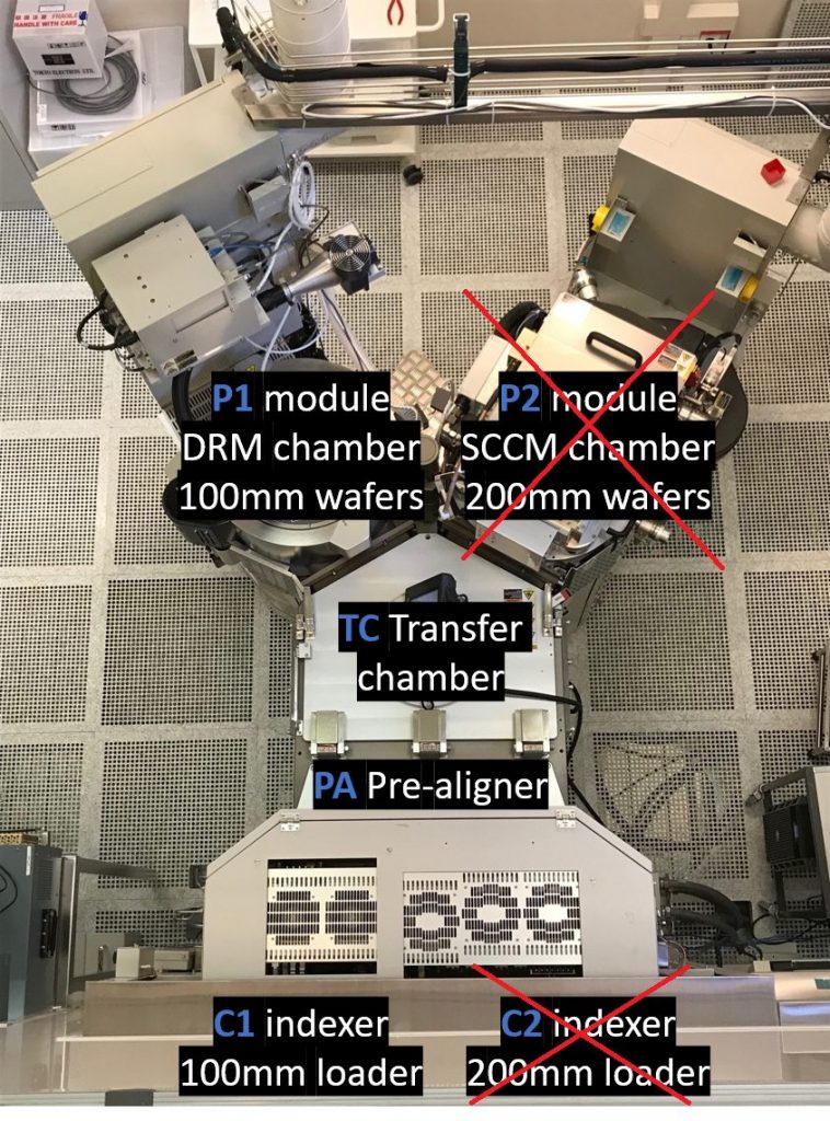
TEL Unity Me system is an automatic plasma etching production tool from Tokyo Electronic (TEL). As shown in figure 1, being available for process at CMi is the cassette loader C1 for 100mm wafers, one transfer chamber (T/C) and the process modules P1 for 100mm, the DRM -Dipole Ring Magnet- chamber. The chamber is dedicated to and its design is optimized for etching dielectrics (e.g. SiO2 and SixNy).
!! C2 cassette loader and P2 SCCM -Super Capacitively Coupled Module- process chamber are not available anymore and are offline !!
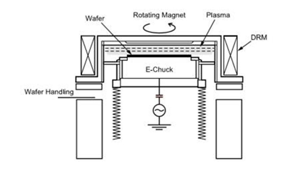
II. DRM chamber for 100mm wafers processing
DRM is a RIE chamber (Reactive Ion Etching) with assistance of a magnetic field. It is structured as shown in the figure 2.
Available process gases: C4F8 [30 sccm], CF4 [100 sccm], CHF3 [100 sccm], CH2F2 [100 sccm], O2 [30 sccm & 1000sccm], N2 [100 sccm], Ar [1000 sccm].
| Materials | Gap (mm) / SH temp (°C) | Process name | Chemistry | Mask material | Etch rate (nm/min) | Selectivity |
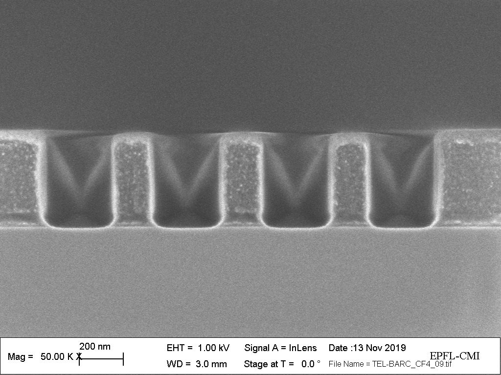
| DUV42P BARC from Brewer | 47 / 40 | CMI.BARC | CF4 | JSR M108Y JSR M35G | JSR M35G DUV42P: 110 M108Y, M35G: 110 SiO2: 170 Si: 85 | 1:1 |
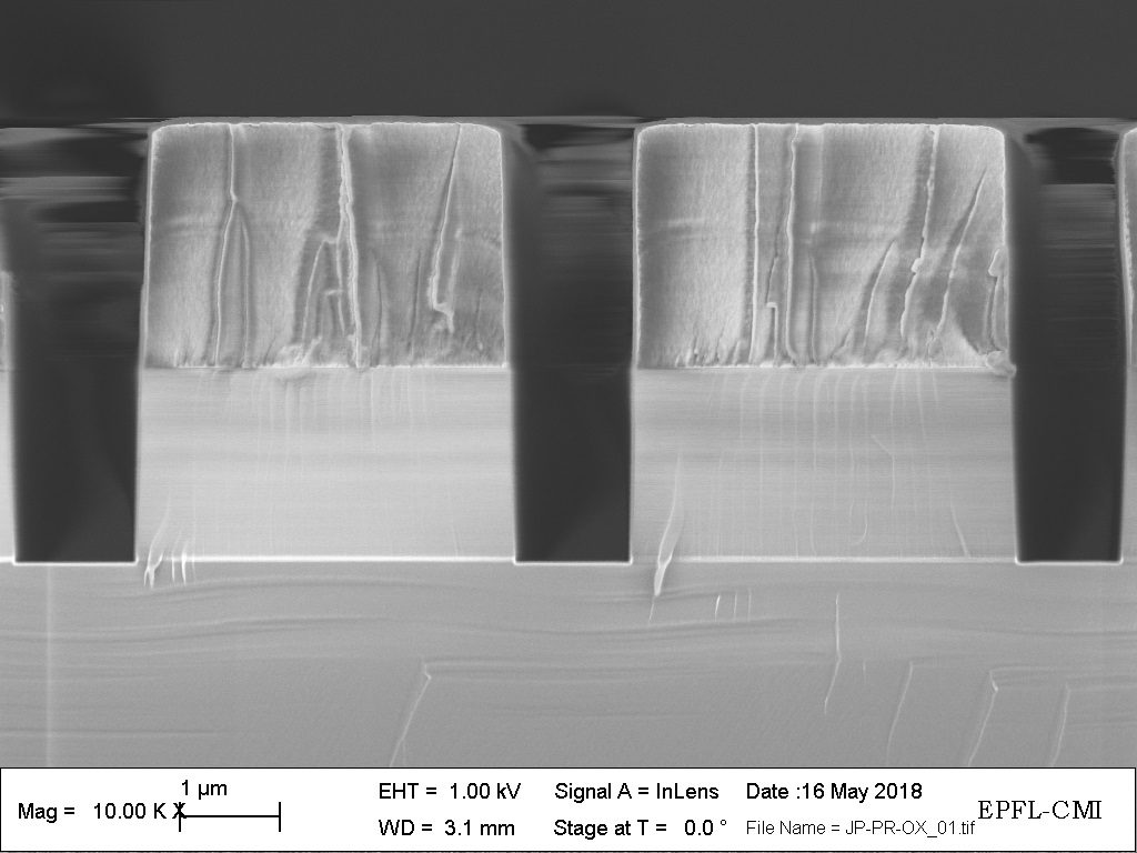
| SiO2 | 47 / 40 | CMI.OX.PR @1100W | C4F8 O2 Ar | PR | SiO2: 415 @600W, SiO2: 230 @500W, SiO2: 200 @400W, SiO2: 160 @300W, SiO2: 125 @200W, SiO2: 85 | >3:1 |
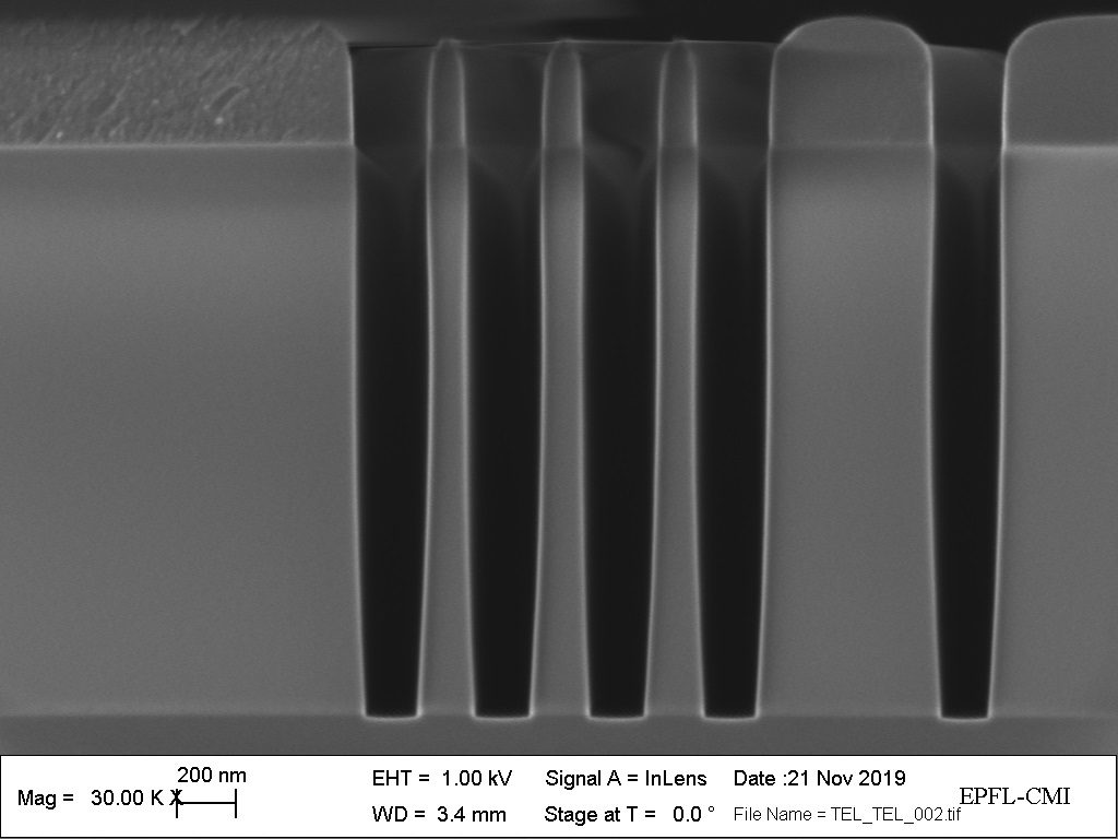
| SiO2 | 47 / 40 | CMI.OX.ASI | CH2F2 C4F8 O2 Ar | aSi | SiO2: 450 aSi: 35 JSR M108Y: 130 | 12:1 |
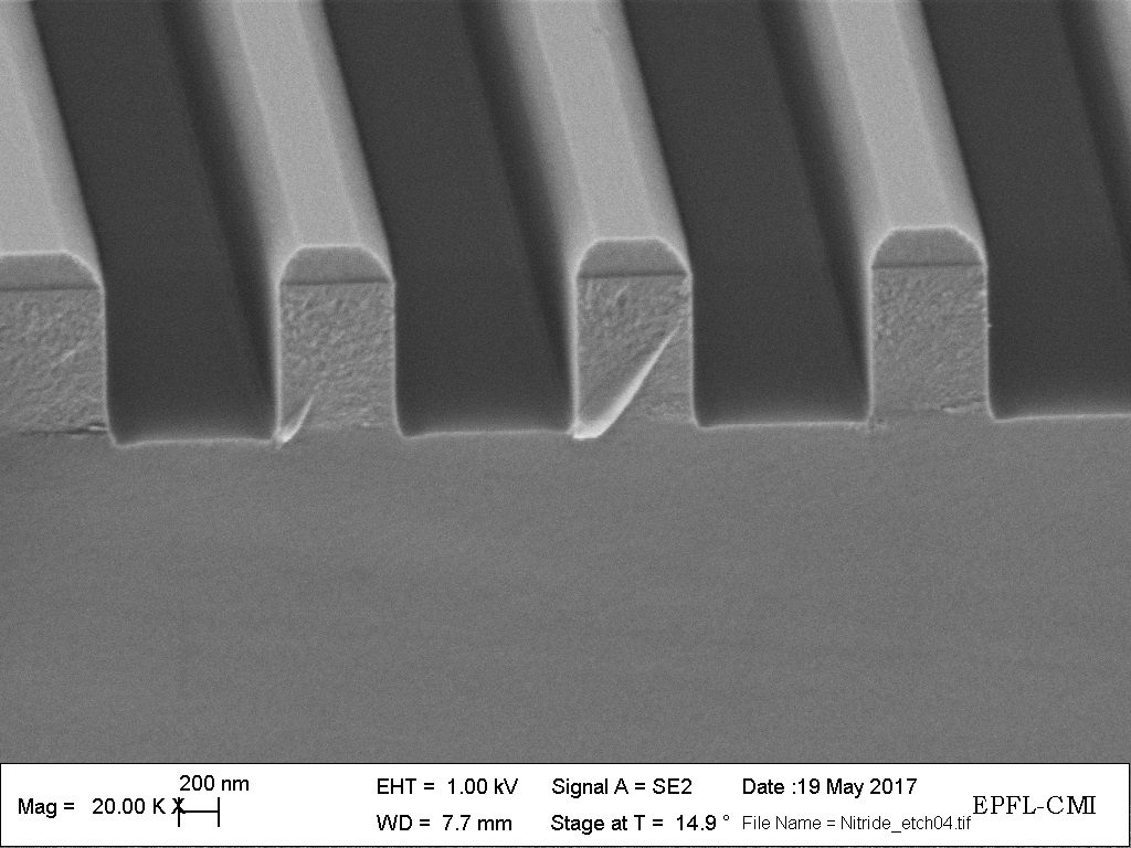
| Si3N4 | 37 / 40 | CMI.SIN.OX | CH2F2 O2 Ar | HSQ PR | Si3N4: 130 Si: 25 HSQ: 80 PR: 125 | >1:1 |
| Chamber Clean | 27 / XX according to etch process | O2/CLN/XXC | O2 | — | — | — |
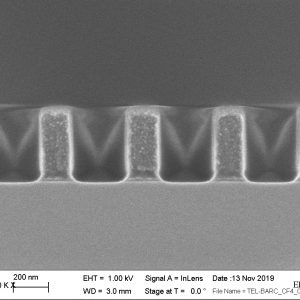
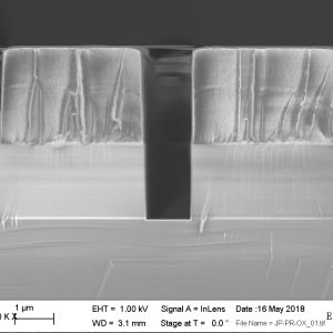
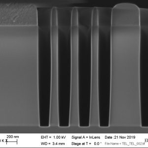
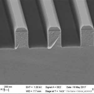
III. Photos gallery