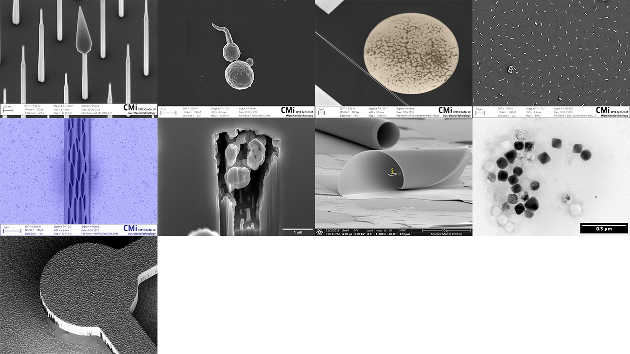
2024, May
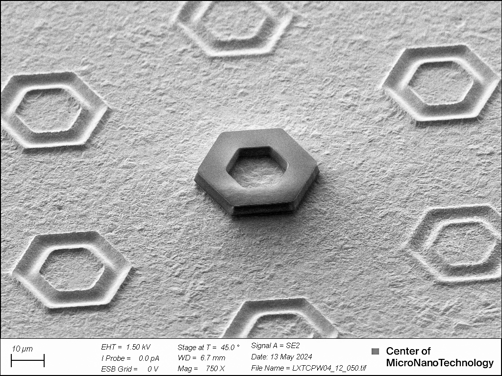
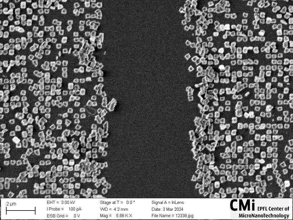
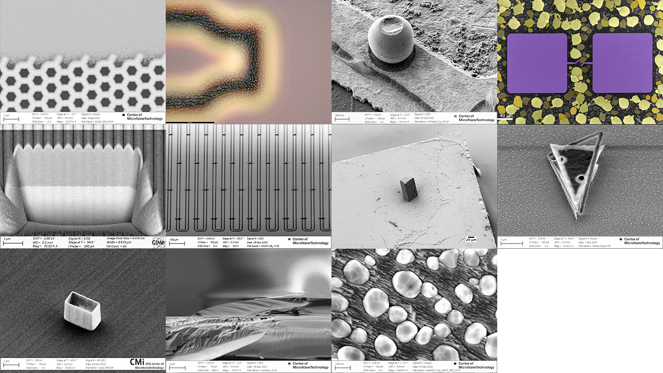
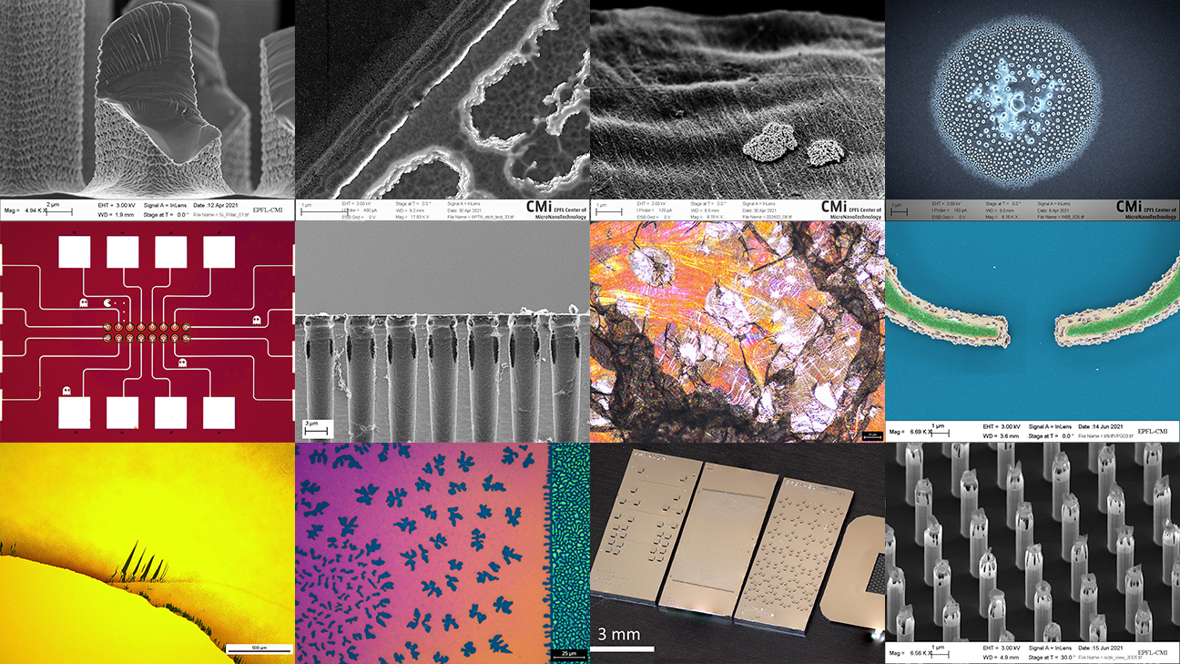
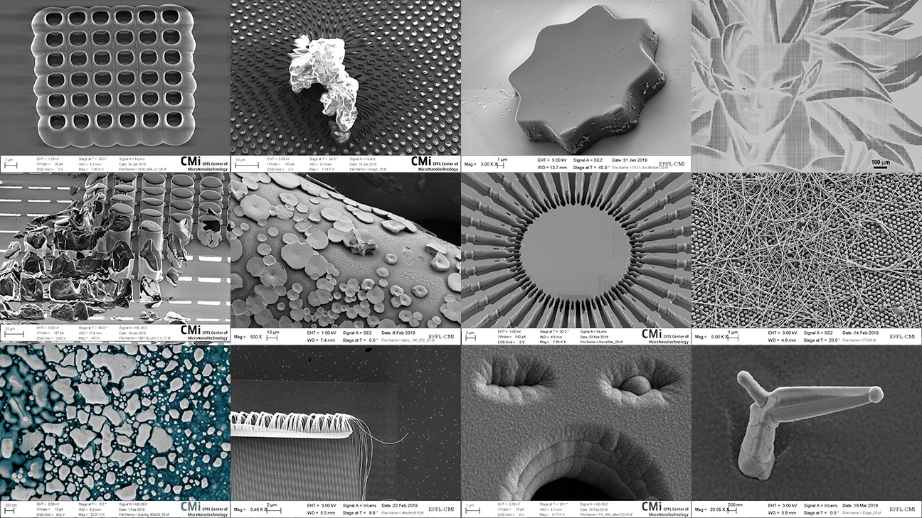
DIY 16um micro-bolts and micro-nuts
Rui Ning Wang, Luxtelligence SA
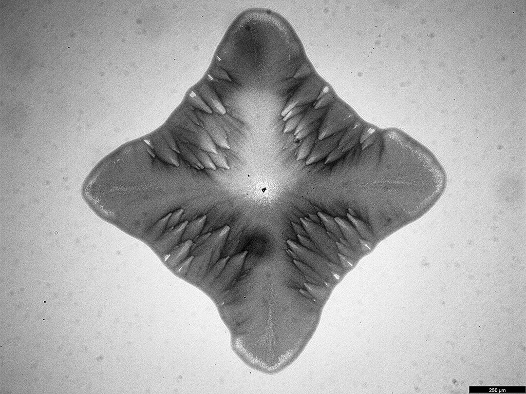
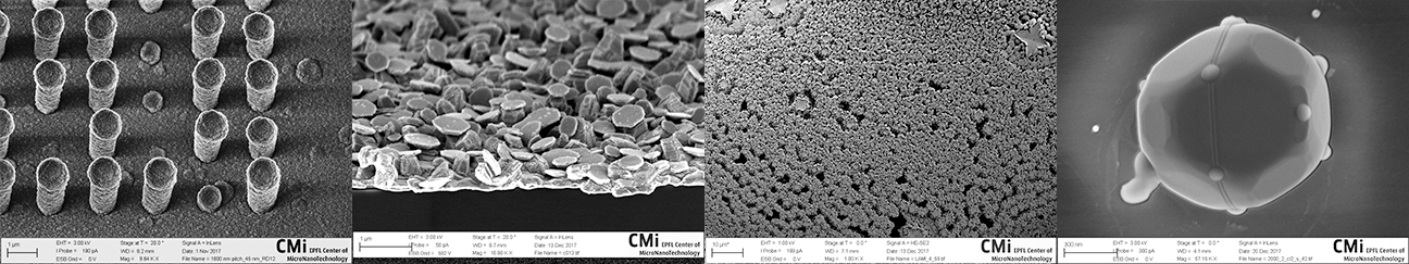
Don’t miss our special deal on these premium micro-nuts, limited time offer only! These nuts are made of ECI3027 photoresist, displayed here on an etched Cu surface. Buy Now! Only few left! (Micro-bolts not included.)
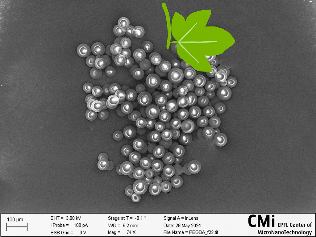
Polymeric Micro-grapes
Tao Zhang, LMIS1
Polymeric micro-grapes are shimmering with a blend of natural artificial beauty, provoking Déjà vu of the wine festival in late May. Microspheres are made of acrylate PEGDA using PDMS-based microfluidics.
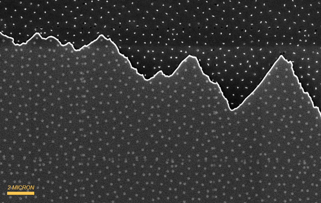
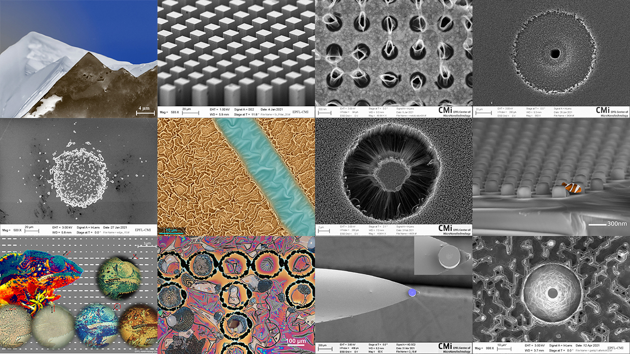
Star gazing in CMi
Anja Tiede, LMSC
The mountain range night sky you can observe here are actually results of a lift-off process of TiO2 nano-pillars (sputtered by DP650) that did not work as intended; scale bar is 2µm. The view even inspired ChatGPT to write a little Haiku: Waiting for ebeam, Process paused, dreams linger on — Mountains ‘neath the stars.
2024, April
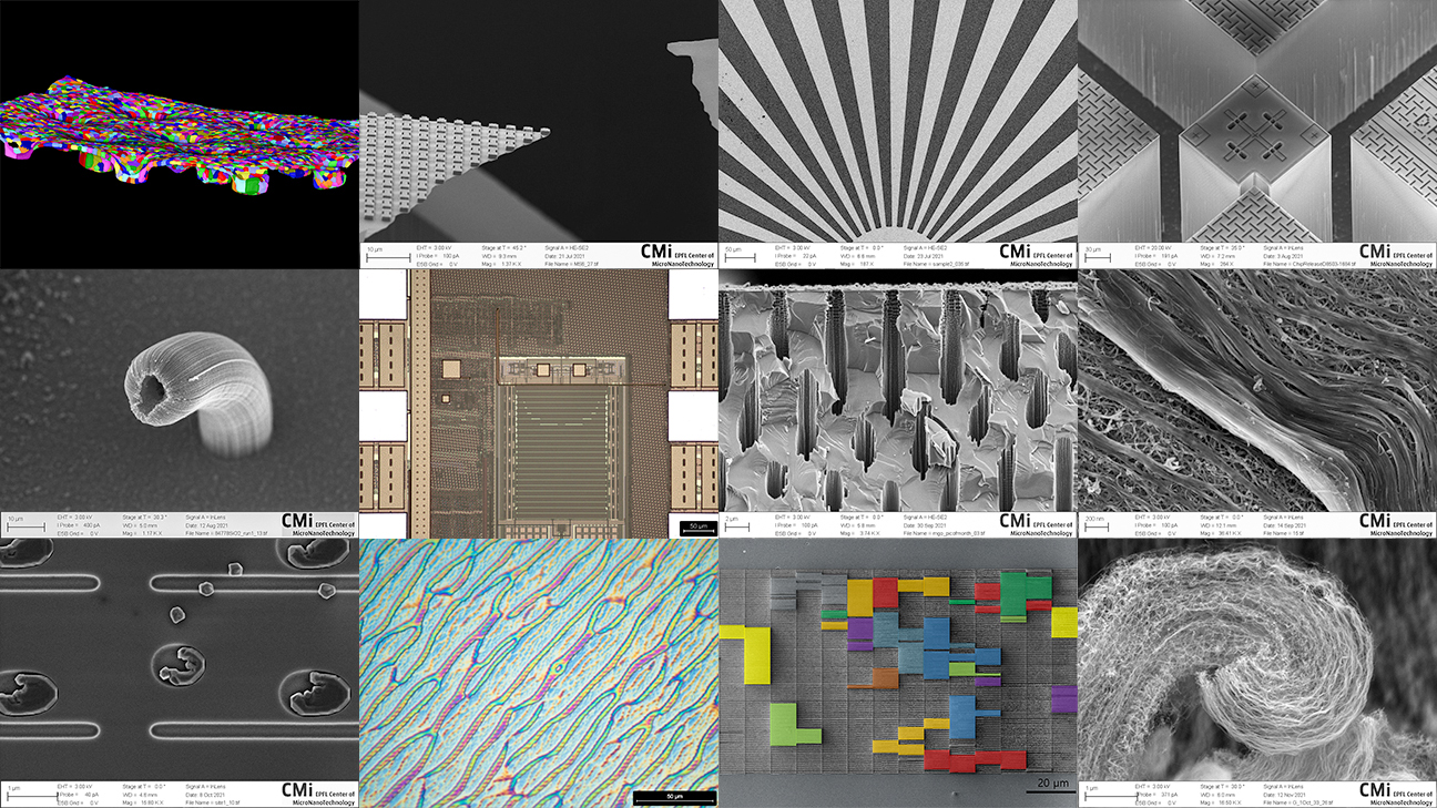
Equiaxed dendritic gold grain
Tecla Bottinelli Montandon, Corintis SA
Particular conditions during anodic bonding sparked the nucleation of defects of gold electrodes to grow in equiaxed dendrites under the borofloat glass. Demogorgon? Weird sea creature? Just a beautiful crystal? You decide!
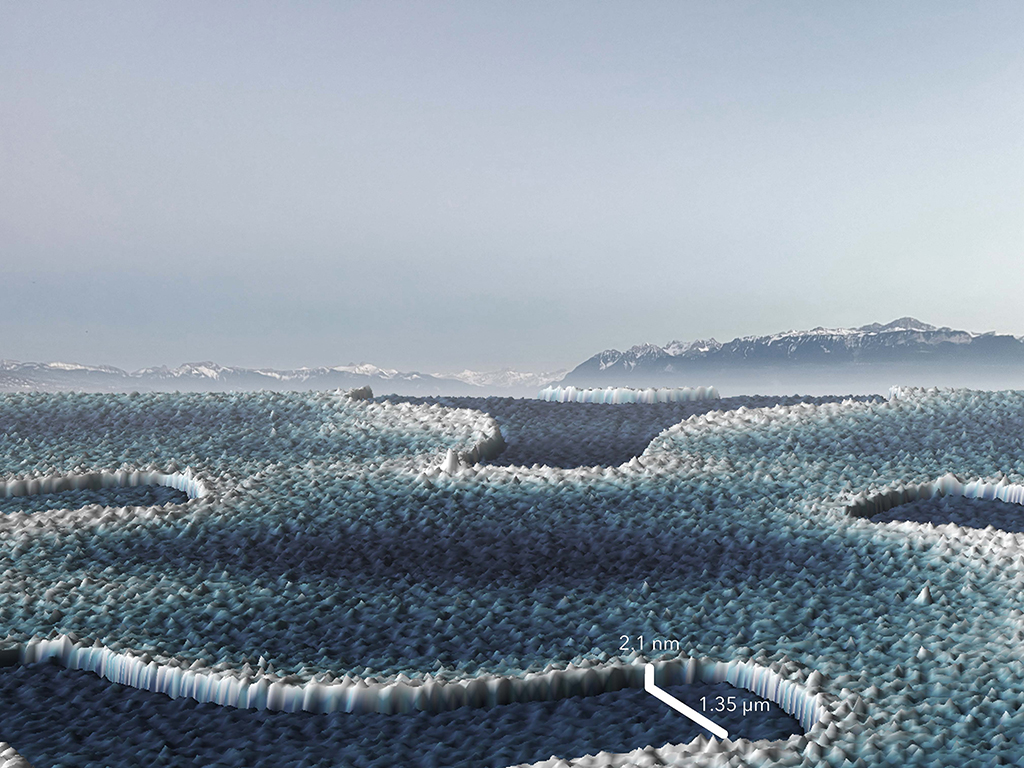
Le Léman 52024!
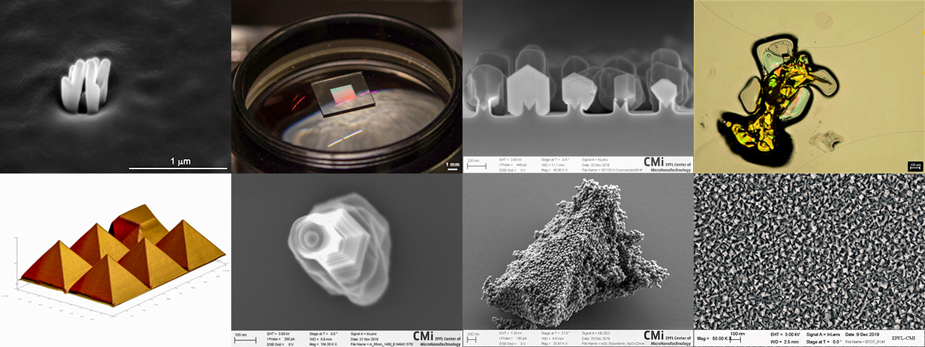
Frantisek Jerabek, LMSC
At CMi, the research pushes boundaries, offering a glimpse into tomorrow. Witness a rare portrayal of Lac Léman in the next Ice Age, captured from Lausanne-Ouchy. The AFM micrograph of Z16 MLA-150-fabricated gold tripods (Z50 EVA 451) embedded in a 25nm SiO2 mask (deposited by Z50 Oxford PECVD, etched by Z02 SPTS APS) was acquired using Z11 Bruker FastScan AFM. Join us on the frontier of discovery, where imagination meets reality.
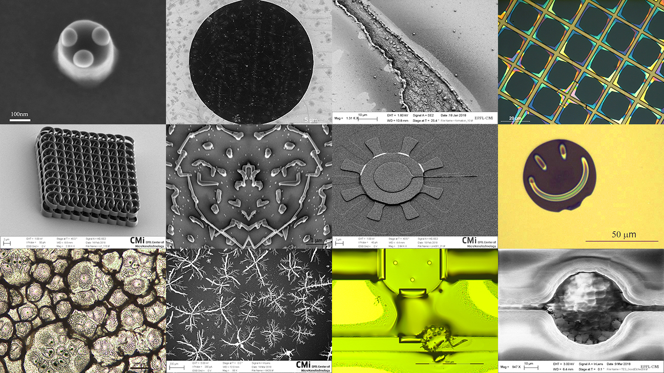
Say “Cheese“
Shelly Ben-David, LMSC
3…2…1… Smile! Your picture is being taken 🙂 The alumina capping on my GeSn microstructures cracked into this camera-lens shape during annealing.
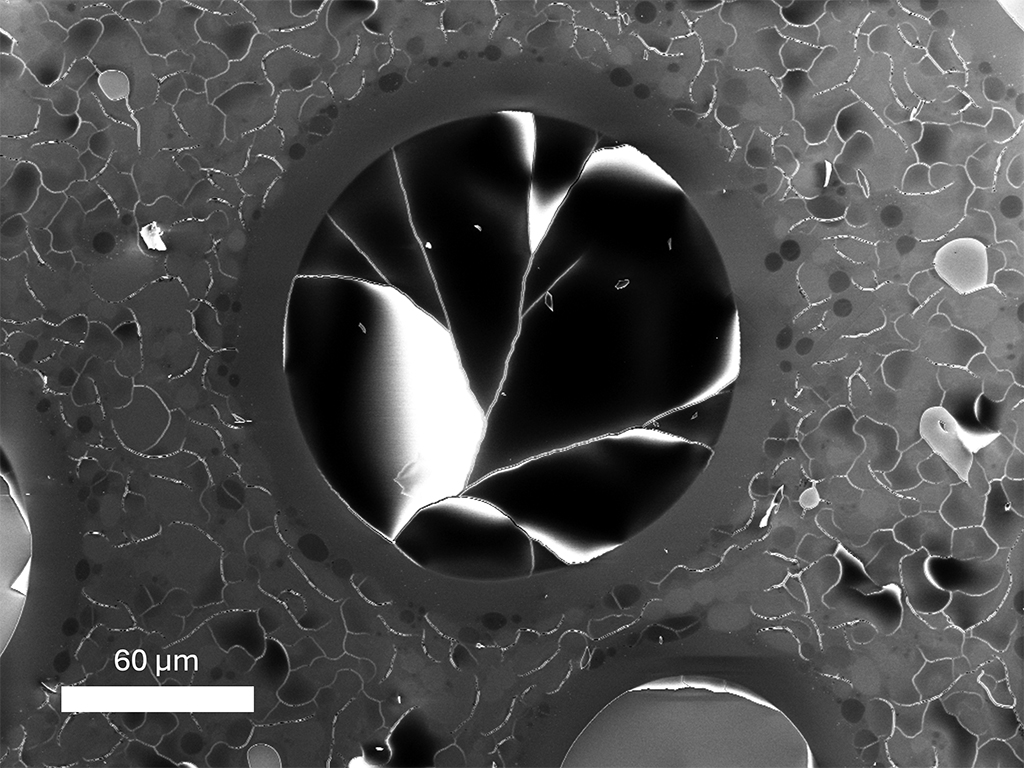
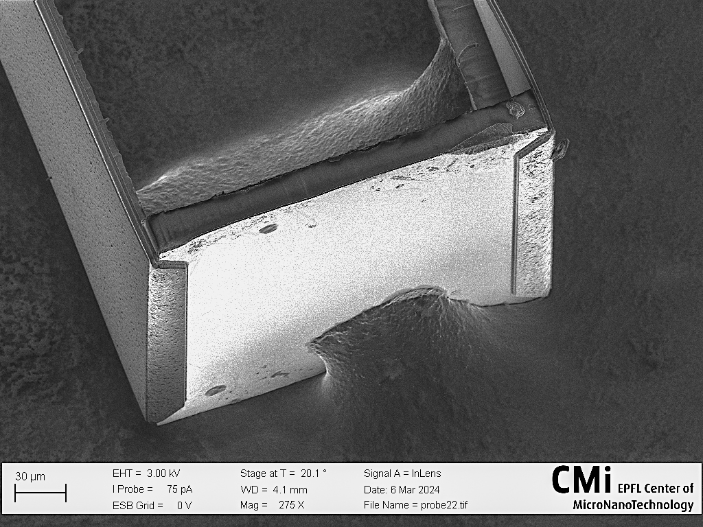
A good looking mistake
Fabian Linus Bauer, NEMS
The image shows needle like structures formed around a release hole on a hafnium carbide thin film after vapour HF release.
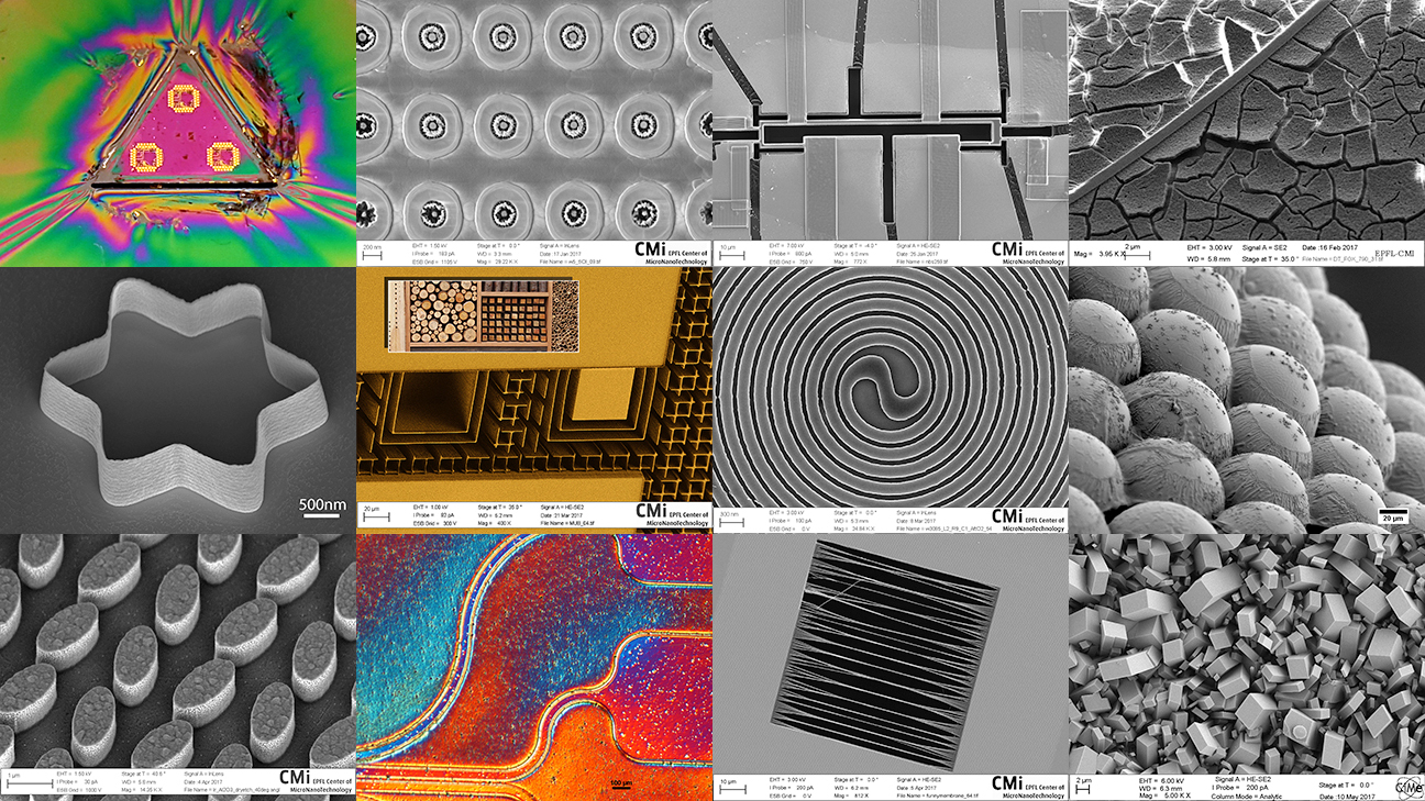
2024, March
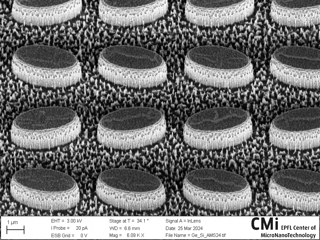
Gothic sidewalls
Ivan Sinev, BIOS
These gothic sidewall motifs were found on a quest for a better etching recipe for germanium. Unfortunately, such architectural sophistications do not go well with the optical properties of the structure.
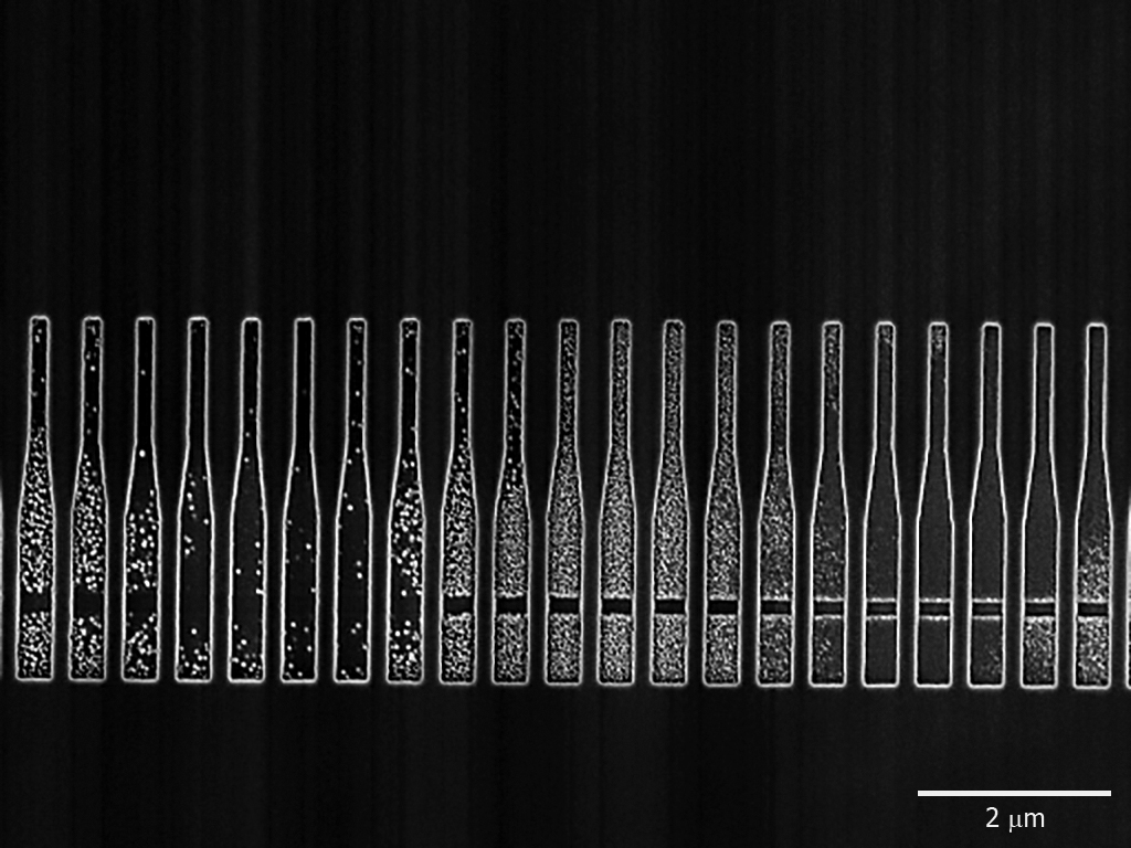
Bottles of wine
Amirhossein Esteghamat, POWERLAB
I hope there is at least one good wine bottle among them 🙂
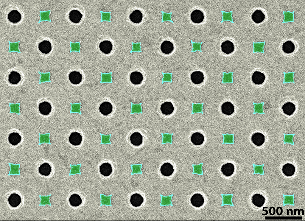
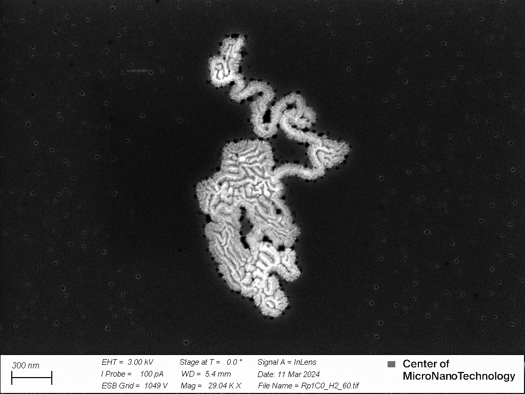
The Interstellar Journey of Plasmonic Black Holes: Remnants of Mysterious Cubes
Wenhong Yang, BIOS
After the IBE350 etching and Tepla 300 Photo Resist (PR) stripping process, astonishing periodic cubes unexpectedly emerge alongside the gold nanohole arrays. These nanocubes seem to have been transported into the nano spatiotemporal realm at CMi through the spacetime teleportation of the plasmonic black hole. Warning: don’t stare at it for too long, or you may end up like the ‘Scale bar’ in the image, transported to unknown territories! This image was captured using a Zeiss SEM Crossbeam.
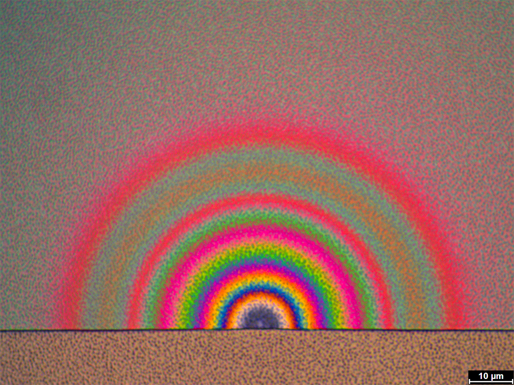
Here comes the (u)sun
Roberto Russo, LMIS1
“Little darlin’, it’s been a long, cold, lonely winter; Little darlin’, it feels like years since it’s been here; Here comes the sun; Here comes the sun”… A small resist contamination unleashed a full spectrum of colors under the microscope!
Pathway towards science
Chufan Zhou, AQUA
The pathway towards science is a journey marked by curiosity, exploration, and rigorous inquiry. It begins with a spark of wonder, a desire to understand the world around us and unravel its mysteries. As we continue along this pathway, we unlock new insights, innovate new technologies, and strive towards a better future for all. TiO2 nano-pillars fall down during the oxygen plasma process.
Neural spacecraft
Melania Coronese, BCI
Did you know that you can go seriously 3D from a slice of silicon wafer which is only 30µm-thick? SEM micrograph of a CMOS-compatible neural probe comprising a pair of Al shanks and a Si chip after planar fabrication and bending to implant configuration.
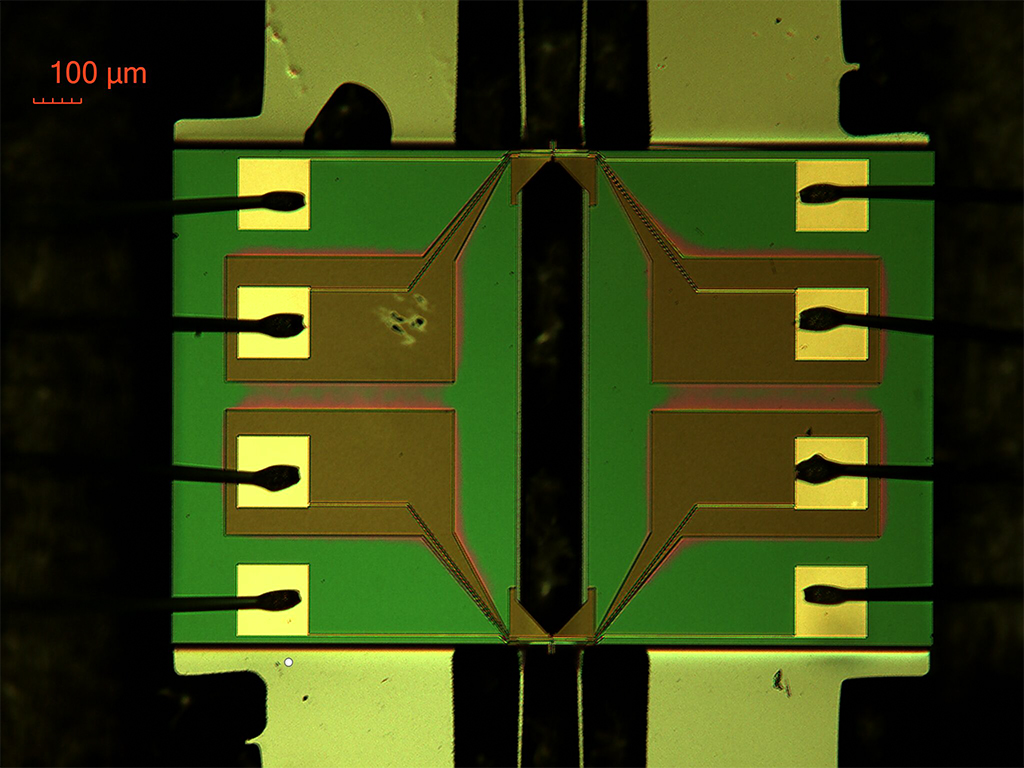
Microtransducers bonded on a PDMS flexible substrate
Hichem Ben Lakhdar, ETH Micro and Nanosystems lab
Wire bonding is always a challenge, in addition to the different force and pressure parameters of the machines that must be found, other complications are to be expected such as the different characteristics of the materials to be bonded as well as their supports. Here tiny squares of Palladium are bonded with a very fine 25-micron Aluminum wire. To complicate the task, this Nanosystems is deposited on a 2mm PDMS substrate which makes it totally unstable when in contact with the needle. Thanks to the expertise of Adrian Toros, we were able to find the exact parameters to carry out the project successfully.
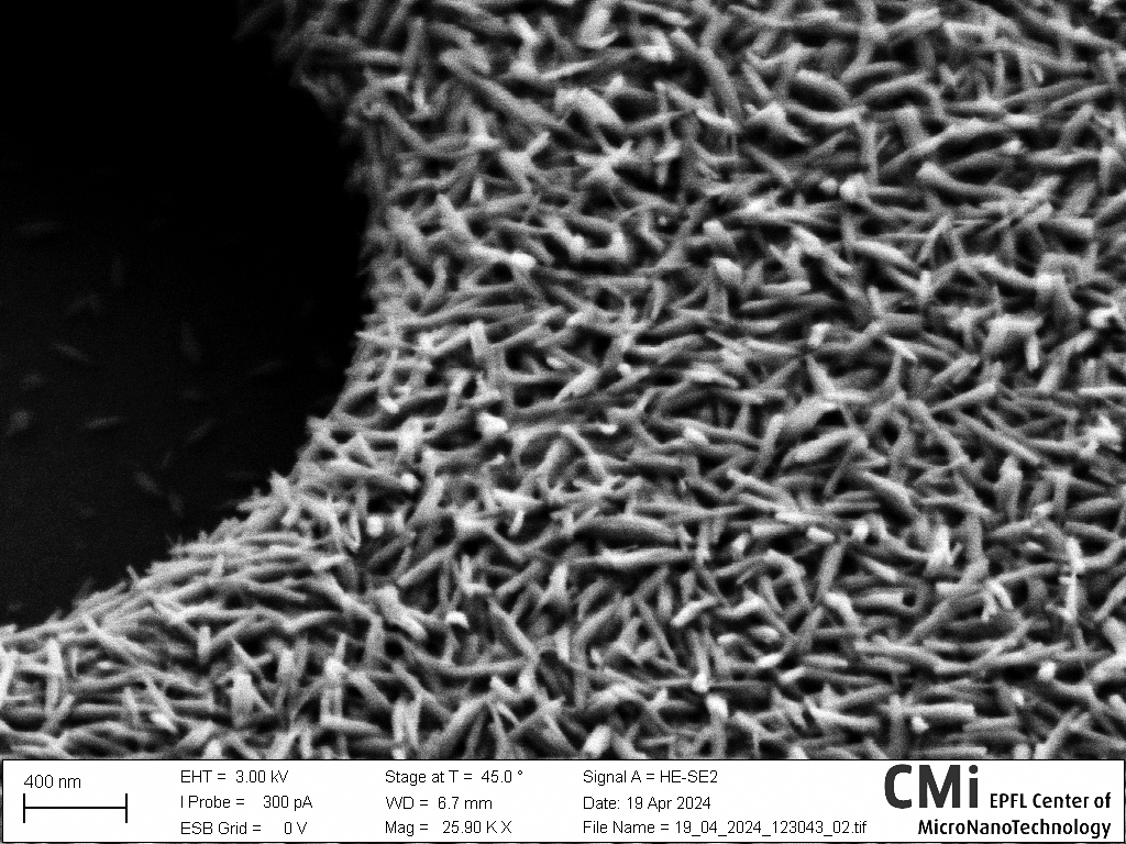
NanoBrain – taking AI to the next level
Hernan Fernando Furci, LMIS1
We have optimized a process to produce NanoBrains on Silicon, a promising gateway to neuromorphic computing and fully integrated AI-on-a-chip. They come with a nanowire spinal cord that could potentially lead to synapses and complex networks. Neural activity measurements show, however, that these brains can be more stubborn than the scientist who produced them.
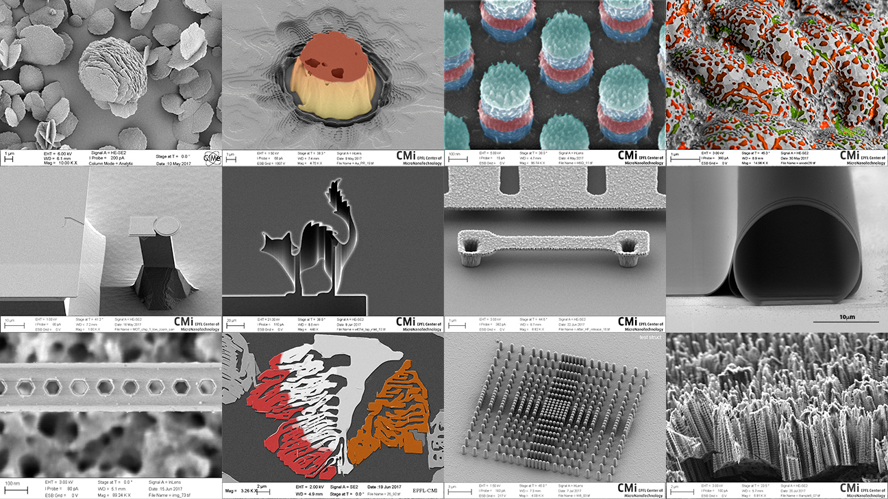
2024, February
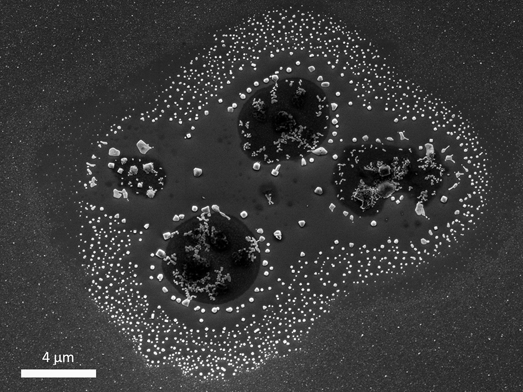
Tropical Nanoislands
Shelly Ben-David, LMSC
Dreaming of a tropical holiday in February? Me too. Join me for an exclusive excursion to these (tweezer-induced contamination) nanoislands in a sea of germanium tin! Price: interest in the science. *Disclaimer: we do not provide trip insurance and the GeSn thin film was sputtered in the DP650.*
2024, January
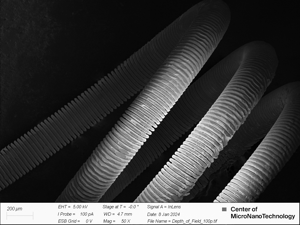
Tungsten filament
Makhlad Chahid, CMi
This is a SEM image of the tungsten filament from the ebeam alignment microscope dead halogen light. To characterize the depth of field of the SEM Crossbeam, I have imaged at different values of Depth of Field. This one has been done at 100%.
2023
2022
2021
2020
2019
2018
2017
2016