To be read first:
- This tool is a MICRO-ELECTRONIC compatible tool :
- No organic layers (Photoresist, Kapton, polyimide etc …)
- No gold and no copper.
RESERVATIONS RULES AND BILLING POLICY :
- Booking : No restriction
- Reservation names must be correspond to operators
- Billing : Processing time + pulse number
- No penalty fees in case of user’s no show
- Below 200C : Booking before 1 am
- Below 300C : Booking after 1 am
- Long time deposition : Night job
CONTENTS :
I. Equipment description
II. Deposition mechanism
III. Layers available at CMi
IV. How to use the system
V. Links
VI. Gallery
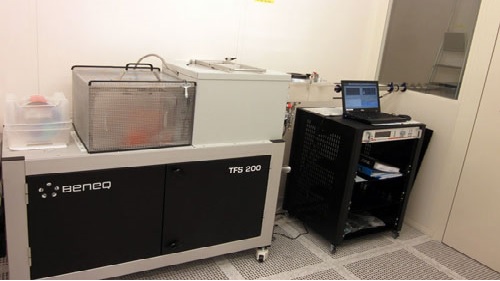
I. Equipement description
The tool Beneq TFS200 is an ALD (Atomic Layer Deposition) system ddicated to the deposition of thin dielectric or metallic layers on wafers from 100 mm up to 200 mm as well as on pieces of wafers. The Atomic Layer Deposition (ALD) technique is recommended for thin layers (30 nm or lower) and/or layers that request a high level of conformality. The deposition is done under vacuum (between 4 to 8 mbar) by pulsing alternatively 2 chemically activ precursors.
The equipment is composed of :
- a chamber with a reactor inside (Temperature 450C max)
- a loadlock system
- 4 liquid sources and 2 hot sources
- 5 gas lines (O2, O3, N2 and NH3 and purge with N2)
- an ozone generator
- a primary pump
The equipment is driven by a software interface but some manual operations are requested for each deposition:
- Chamber and/or precursors heat up
- Loading and unloading the samples
- Opening of the liquid precursors at the beginning of the process
- Closing of the liquid precursor at the end of the process
II. Deposition mechanism
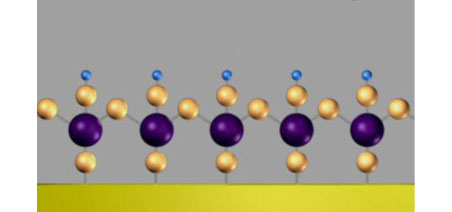
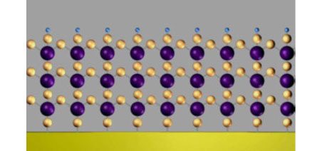
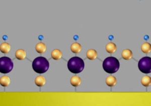
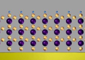
The mechanism of deposition for the Atomic Layer Deposition (ALD) is composed of 4 steps as described below whatever the reactor:
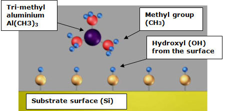
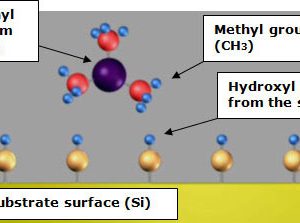
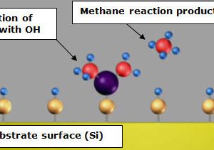
- The first precursor (precursor 1) is pulsed into the reactor and reacts at the surface of the sample by chemisorption to form a monolayer.
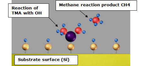
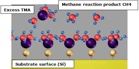
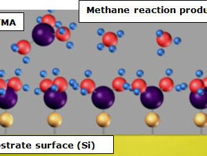
- The reaction chamber is purged with inert gas (N2) and the excess of precursor 1 is removed.
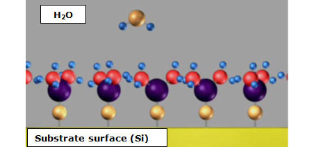
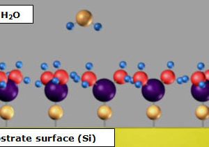
- The second precursor (precursor 2) is pulsed into the reactor and reacts with the precursor 1 already present at the surface of the sample. The reaction generates the desired monolayer and a byproduct.
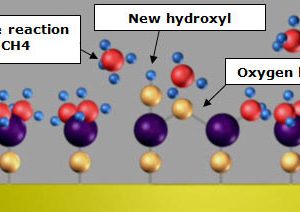
- The byproduct and the excess of precursor are then purged from the reactor with inert gas (N2) (step 4).
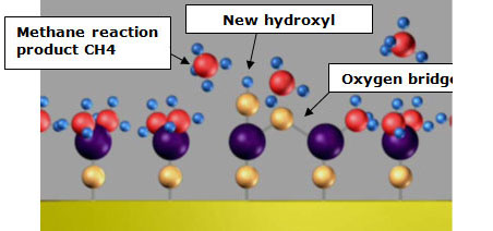
The 4 steps represent the elementary loop which is repeated until we get the requested thickness of the layer. An illustration of these 4 steps is done with the deposition of Al2O3 from the Tri-Methyl Aluminum (TMA) and water (H2O).
III. Layers available at CMi
In the table below, the list of the layers available at CMi with standard process conditions. In comments, below the table, specific informations and comments regarding each layer.
| Layer |
Precursor 1 |
Precursor 2 |
Chamber temperature (°C) |
Deposition rate (A/cy) |
| Al2O3 | TMAl – RT | H2O | 80 – 300 | 1.15 +/- 0.05 |
| Al2O3 | TMAl – RT | O3 | 80 – 300 | 1.15 +/- 0.05 |
| TiO2 | TiCl4 – RT | H2O | 80 – 200 | 0.42 +/- 0.05 |
| TiO2 | TiCl4 – RT | H2O | 250 | NA |
| HfO2 | TEMAHf – 80°c | H2O | 200 – 300 | 1.01 +/- 0.05 |
| SiO2 | BTBAS – RT | H2O | 300 | 1.01 +/- 0.05 |
| Pt | (CpMePtMe) – 75 °c | O2 | 280 | 0.5 +/- 0.05 |
*The deposition rates are given for a deposition temperature of 200°C
For TiO2 layer, the layer’s phase changes at around 200°C. Below 200C, the layer has a low roughness. Above 200°C, the layer is very rough.
HfO2 : Hot source heating time 45 min.
SiO2 : Cycle time relatively long, night job is recommended for a layer thicker than 50 nm.
Pt : Hot source heating time 45 min. Deposition very expensive 10 nm : 350 CHf for EPFL users !
IV. How to use the system
V. Links and references
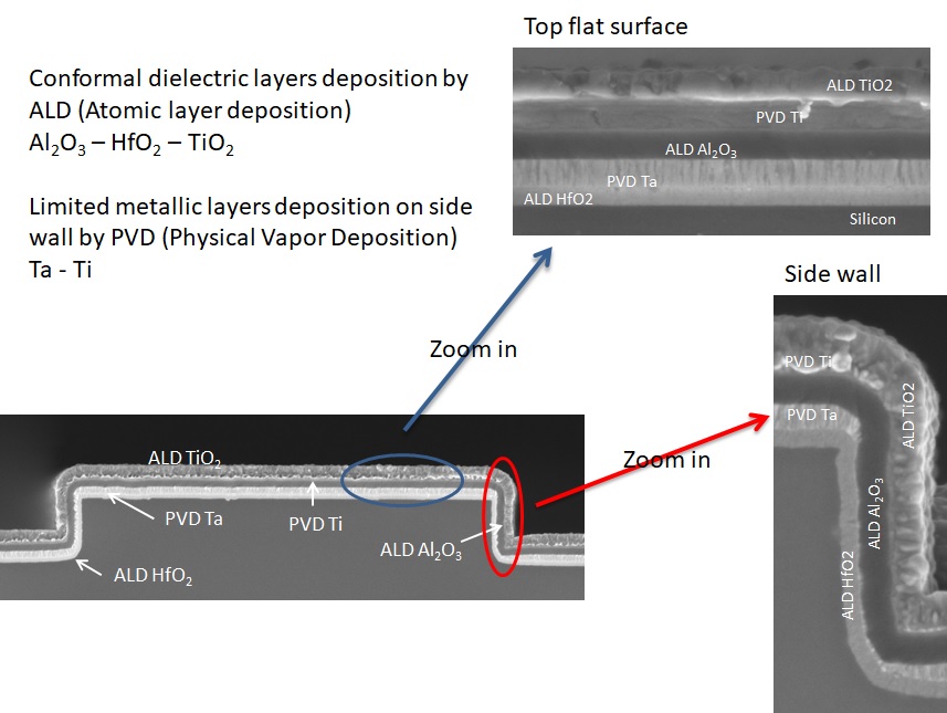
VI. Gallery