Back to the current year Winners
2023, December
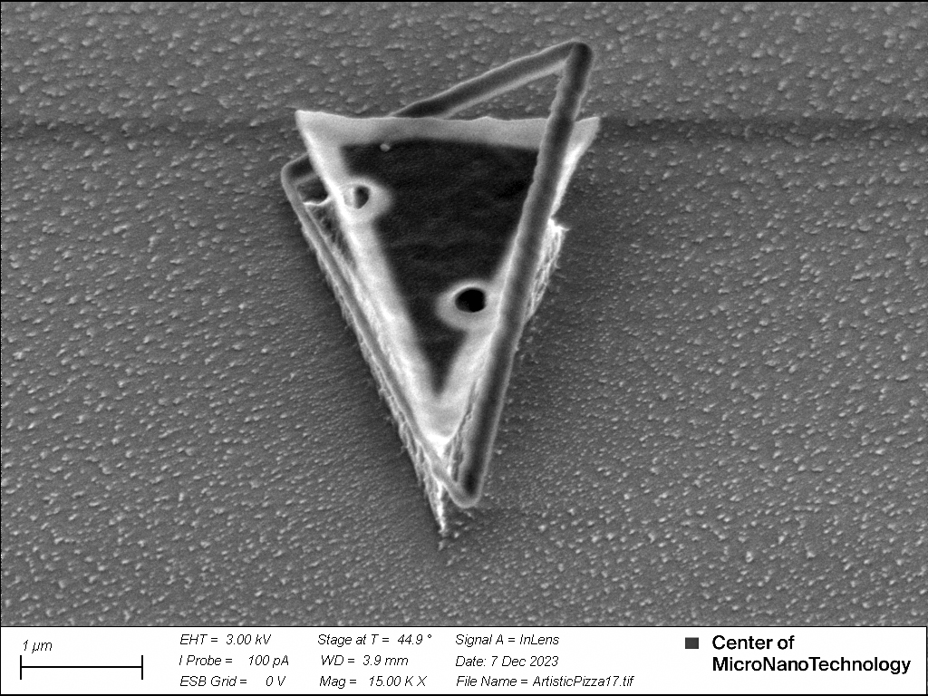
Dolce far Niente
Yuchun Zhu, LQNO
Here comes another one: “artistic pizza slice”, Dolce far Niente for the upcoming Christmas season. It also looks like a piece of cheese, maybe I should have colored it in yellow.
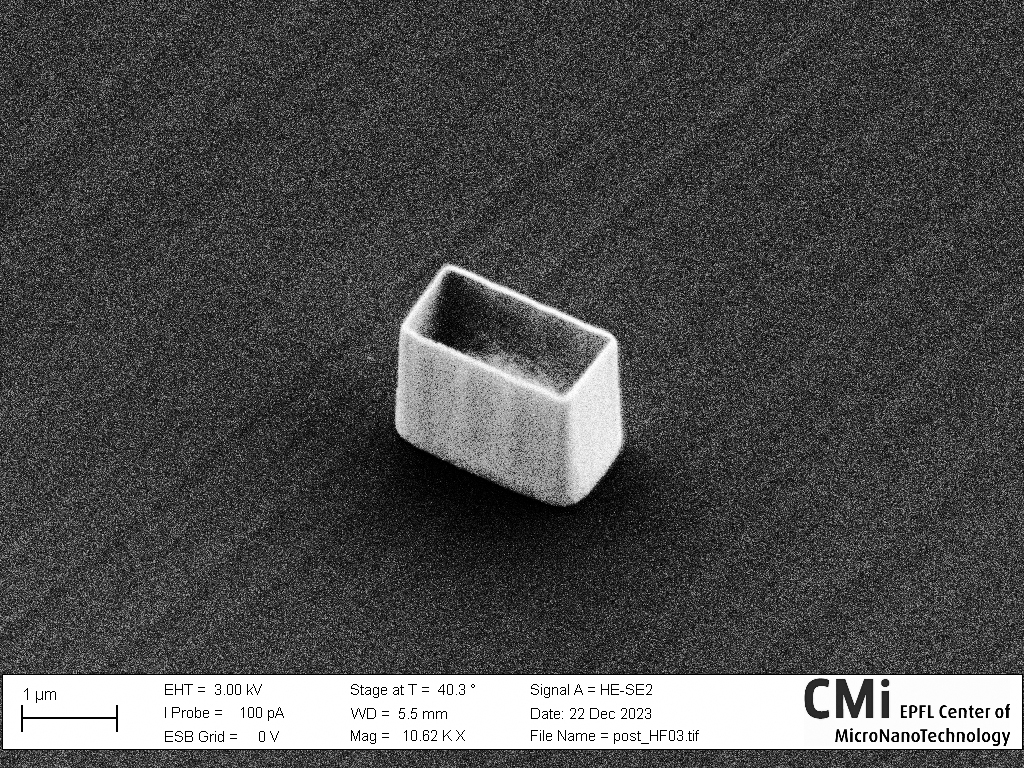
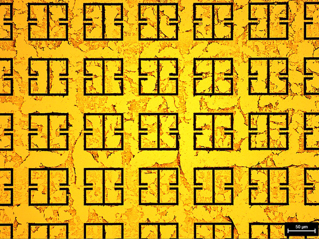
New year’s gift
Kexin Wu, LQNO
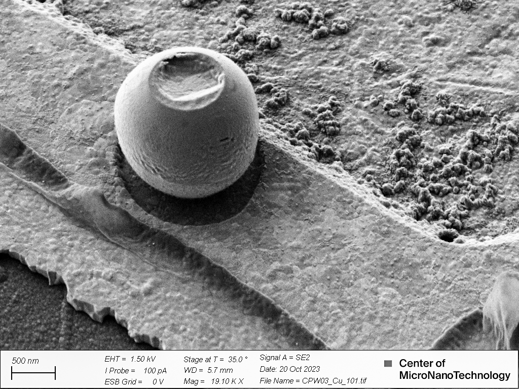
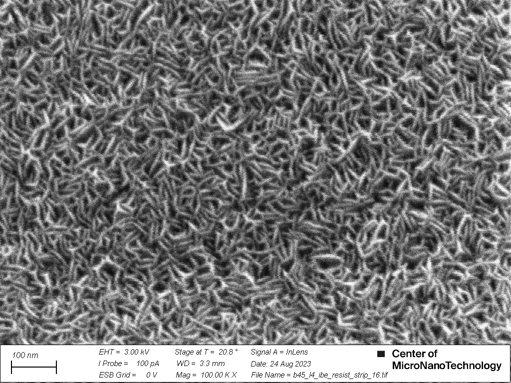
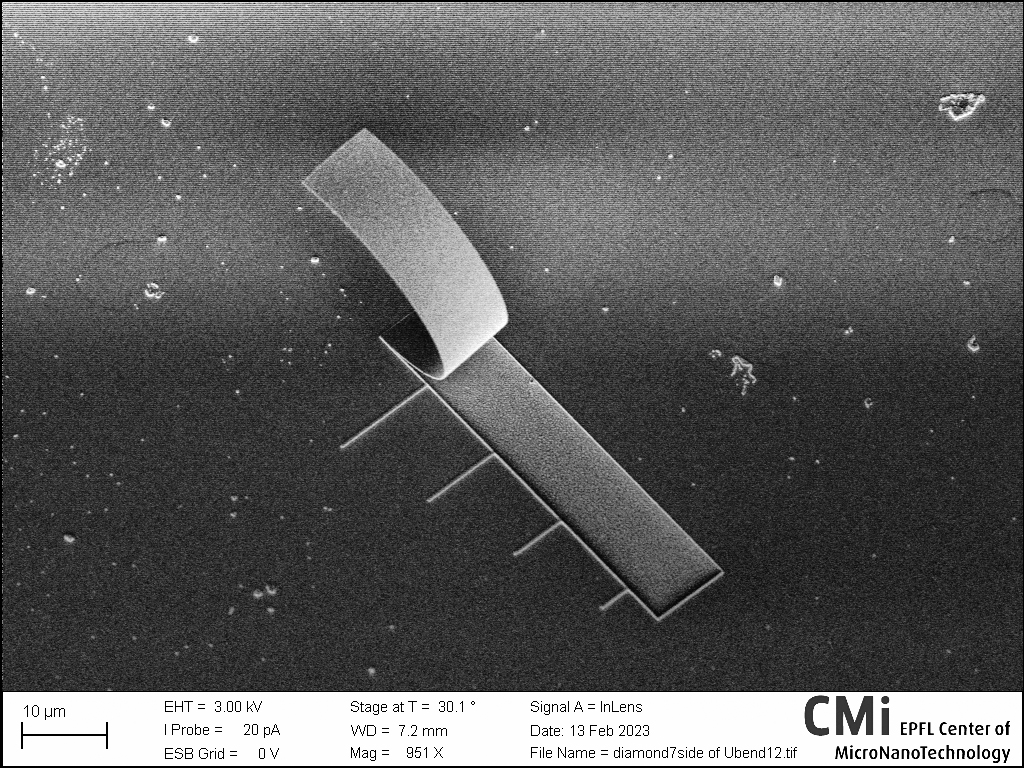
Purely gold made box on the diamond substrate is irresistible to open. Au was redeposited on the sidewalls of developed HSQ during IBE, after the dip in HF, pure gold box was formed (confirmed with EDX).
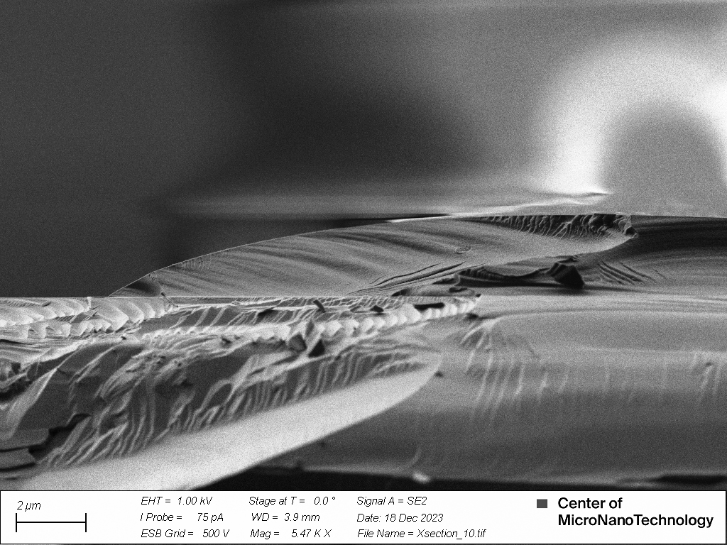
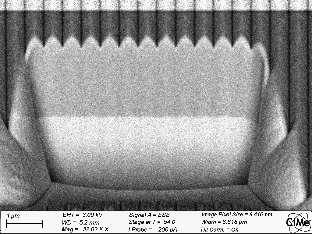
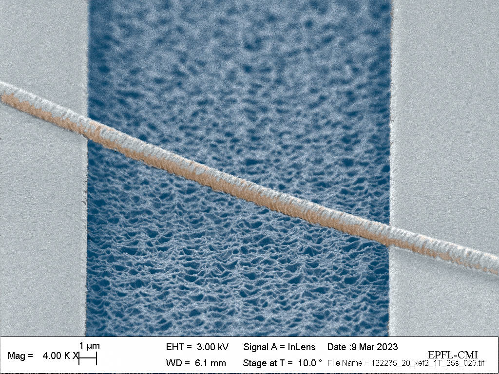
Dunes
Elena Acinapura, HQC
Cross-section SEM image of a cleaved chip with photoresist on top. The photoresist has acquired the tapered profile visible in the image thanks to reflow on a hotplate after opening some windows with photolithography. This tapered shape, in addition to the irregularities given by the chip cleaving, reminds us of desert dunes.
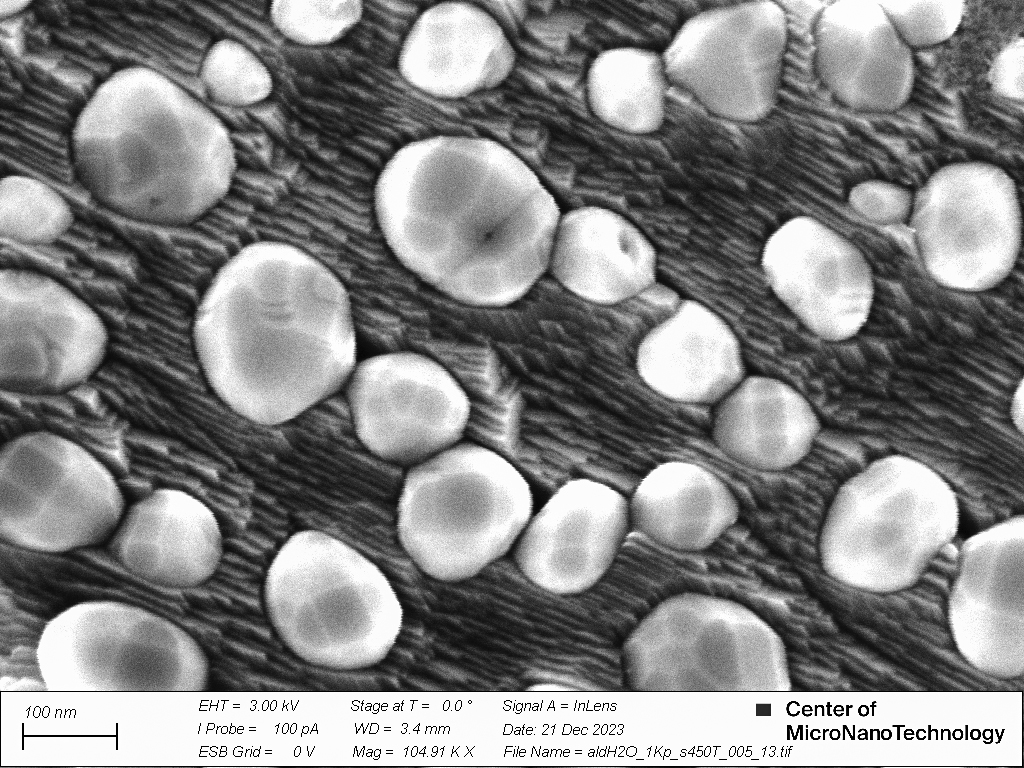
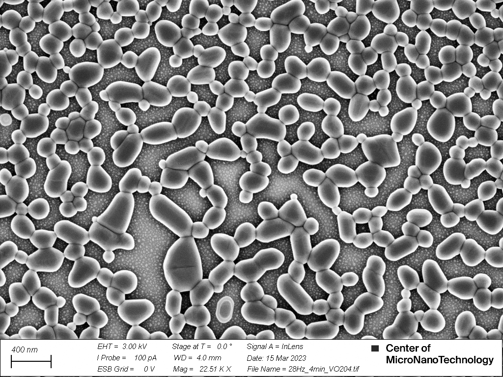
Solidified lava
Anna Varini, Nanolab
This reminds me of Icelandic lava that got solidified as it was flowing around nano-rocks of VO2.
2023, November
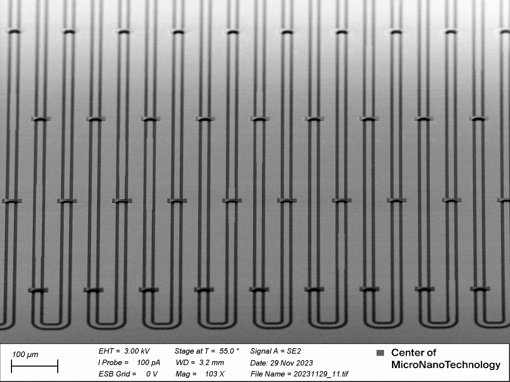
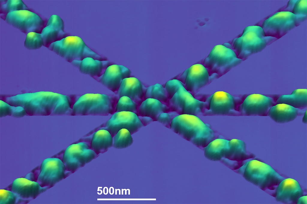
Aluminum airbridges
Hao Li, LPQM
Hundreds of aluminum airbridges connect the ground of the Niobium coplanar waveguide, which is more than half a meter long.
Lonely out of nowhere
Buse Ünlü, LAPD
A building-like structure is fabricated spot-by-spot and layer-by-layer through the 2-photon polymerisation method where a photosensitive resin undergoes a chemical reaction and changes its phase from liquid to solid upon light absorption followed by polymerization.
2023, October
Unidentified micro-blueberry
Rui Ning Wang, Luxtelligence
Sometimes, while taking a leisurely stroll along one of your freshly fabricated gold contact pads, you might encounter an unidentified wild variety of micro-blueberry. These berries do look very tasty, but I’m not 100% sure they are actually edible.
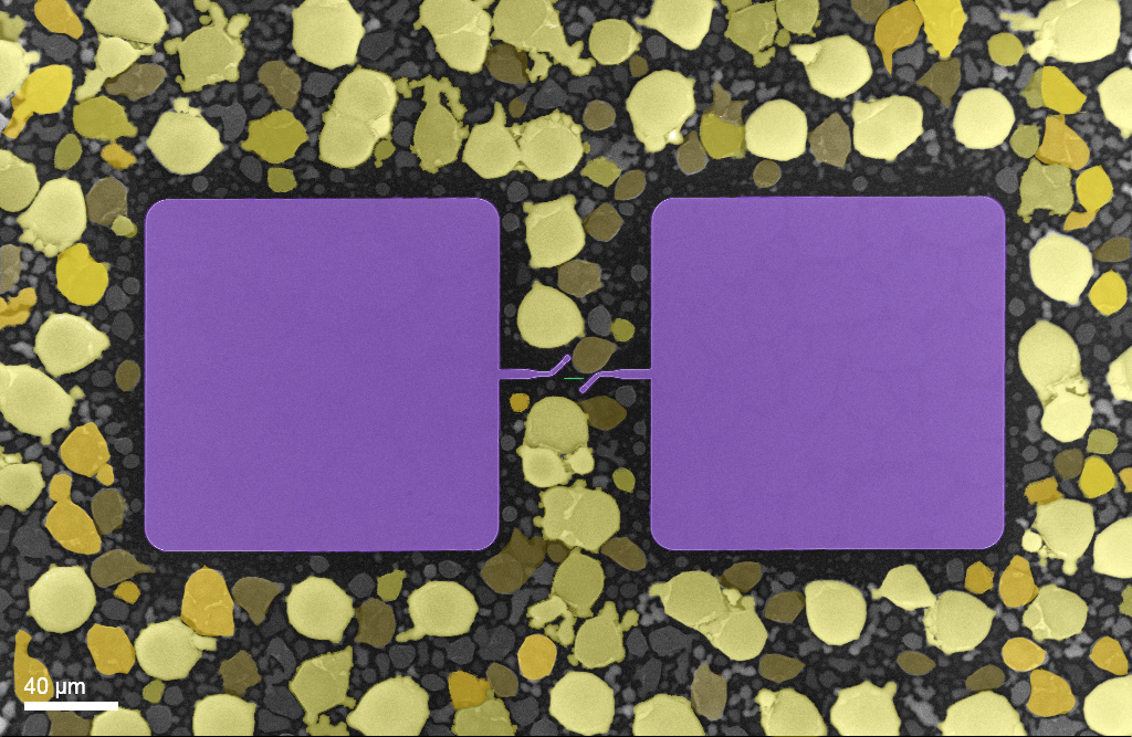
Nano-Ginkgo Leaves
Xuxin Wang, LPQM
The SEM image shows Niobium electrodes (purple) of a dummy pattern of transmon qubit surrounded by residual e-beam resists resembling ginkgo leaves (yellow). A thin Aluminum wire (green) is directionally evaporated using Plassys UHV evaporator, before which a step of 1% HF dipping is added to clean the interface between Niobium and Aluminum. The HF liquid somehow damaged the PMMA/MMA resist and produced flakes of residual resist. Same issues have already been reported in a similar image in the honorable runner-ups section of the September 2023 “Picture of the Month”.
Glass Saw
Mahmoud Abouelatta, NAM
FIB cut for triangular pattern of ridges which are fabricated first on a Silicon wafer, and are then thermally oxidized to obtain this glass saw on the top of the silicon substrate.
2023, September
Wet etching
Igor Golovchanskiy, SQIL
The picture shows a 3D transmon on Si substrate fabricated as a trial in CMi facility using e-beam lithography, Plassys shadow deposition, and wet etching of the substrate. At a certain point of development of our fab routine we decided to try an additional wet etching step of the sample after the lithography and before the Al deposition. Surprisingly, this step resulted in erosion of the e-beam resist by creating a though-holes all over the surface, except of the edges of the pattern. Thus, subsequent deposition of 60 nm of Al leaves metal blurs on Si surface. Interestingly, blurs in proximity of the pattern are clearly smaller than the others, which indicates some tricky kinetics of the chemical process.
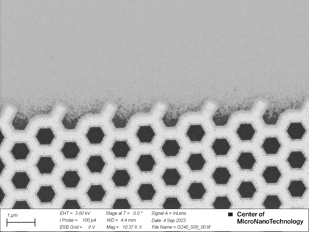
Nanocosmic Whispers: Hexagons and Celestial Breezes
Seyed Alireza Hashemi, LMIS1
In this SEM image, a story of contrasts emerges. Hexagonal islands command geometric grace in the lower reaches, while an endless plain stretches above. At their juncture, hexagons yield, becoming cosmic stardust carried on an unseen celestial breeze. Amidst these hexagonal islands, elliptical treasures nestle in the trenches, an unpredictable nanoscale waltz. Hexagons surrender, in celestial sway. Becoming stardust, they gracefully fade away. Among these islands, elliptical treasures lay. In the trenches, they waltz, in the nanoscale’s play. In this world of contrasts, where secrets lie. A masterpiece emerges, beneath the endless sky.
Weathered leather
Ekin Asım Ozek, LBNI
Amid the cosmic theater, a tactile tableau unfolds on silicon, painted by the precision of SF6 etch chemistry. The canvas, a medley of SiN’s shiny hues, Si’s intrinsic shades at etch pit, and the almost ethereal transparency of photoresist, manifests a surface reminiscent of weathered leather.
2023, August
Pan-fried noodles
Nan Xu, NEMS
The fresh CMi made ‘pan-fried noodles’ are coming.
2023, July
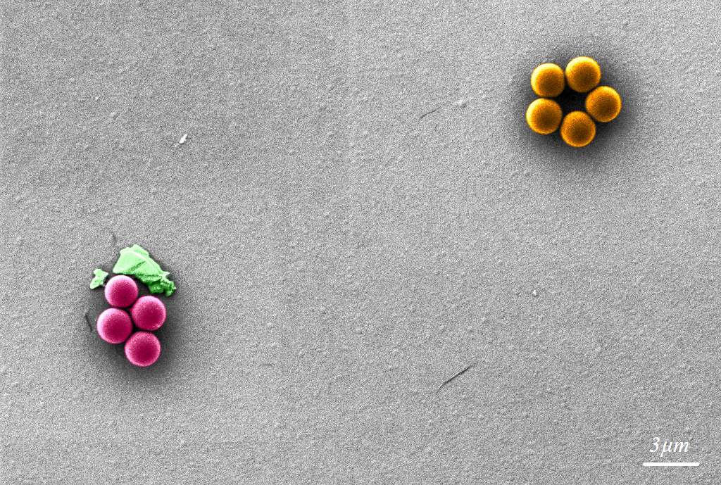
Polystyrene Art
Yara Abdelaal, NEMS
A great drawing starts with simple circles and straight lines. During the examination of a dried droplet of a polystyrene beads’ solution, it was found that the beads assembled to form a beautiful flower and – with the help of residues – grapes; two essential elements of still life painting. This image was taken with the Zeiss SEM Crossbeam at 3kX magnification.
Micro-mushrooms
Michel Jeanneret, Aleva Neuro
What could be better than micro-mushrooms for a micro-fondue? Forks and fondue pot will be ready for this winter. The mushrooms are made of 7.8um-thick polyimide and were immortalized by the SEM Merlin.
Ancient message
Daniil Riabov, BIOS
EPFL community, I desperately need professional decoder! It seems that some ancient tribe left a message on my Silicon chip! Yes, some people want to convince me that it’s just a bad influence of proximity effect in my ebeam job. But how the circular nanogroove array could turn into this?? I don’t believe! Please, respond…
2023, June
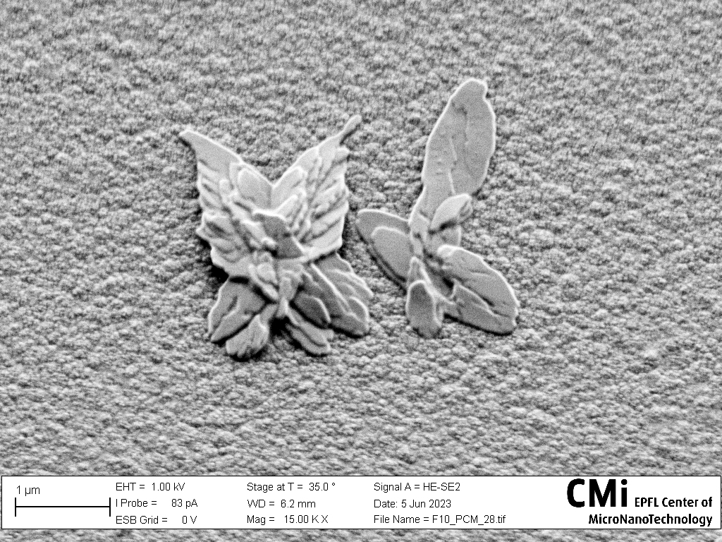
Look there is a butterfly on our chip!
Ozren Petrovic, Ligentec
Defectivity is a common issue we all fight against. At times, it presents itself in beautiful and unexpected patterns.
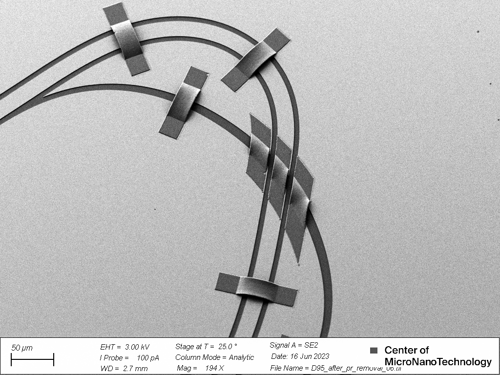
A highway on the microscale
Mikhail Churaev, Viacheslav Snigirev, LPQM
Aluminum air bridges used as interconnects for niobium microwave integrated circuit elements on a thermal oxide wafer.
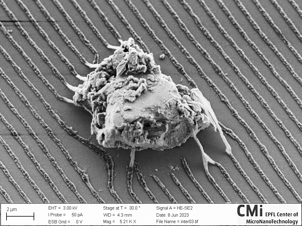
Suspended bridges
Vittorio Bonino, HYLAB
The exposure of an electronic resist through Electron Beam Lithography is incredibly effective. It allows transferring a specific pattern onto the surface, even with very small dimensions, thanks to the ability to focus the electrons in a highly confined space. In this case, the resist settled on a residual crystal from a previous process step, and when it was exposed, it created “suspended bridges.” It can also be observed that on the sides of the crystal, the electron beam was deflected, transferring this disturbance to the final pattern. No, it’s not a strange alien cocoon.
Polymer dam
Augoustina Maria Economou, LBNI
It only takes a thin line to separate abstraction and chaos from order and silence. Often times, the former state is far more fascinating and vibrant than the latter. Here the polymer BCB which was spin-coated on a silicon wafer with a thin nitride film is delaminating around a dry-etched microfluidic mixing design. The image was taken with an optical microscope in the CMi.
Micro El Dorado
Vittorio Bonino, HYLAB
Gold is widely used in micro and nano fabrication, not because it is beautiful and shiny, but because of its high electrical conductivity. In this case, it has been used to create a metasurface made up of LC antennas. Although a sufficiently thick layer of gold absorbs and reflects terahertz radiation completely, these antennas are capable of re-emitting the radiation through the surface, making it almost completely transparent for specific wavelengths. What a satisfaction when a device works, especially if it shines like El Dorado!
2023, May
Germanium jam in the junction
Joel Reñé Sapera, LMSC
What is in the picture? The junction was created with a process of lithography to open slits on a SiO2 mask. Later the germanium was grown with MOVPE, only attaching inside the slits and forming NWs. The image was taken in the Bruker FastScan AFM of zone 15.
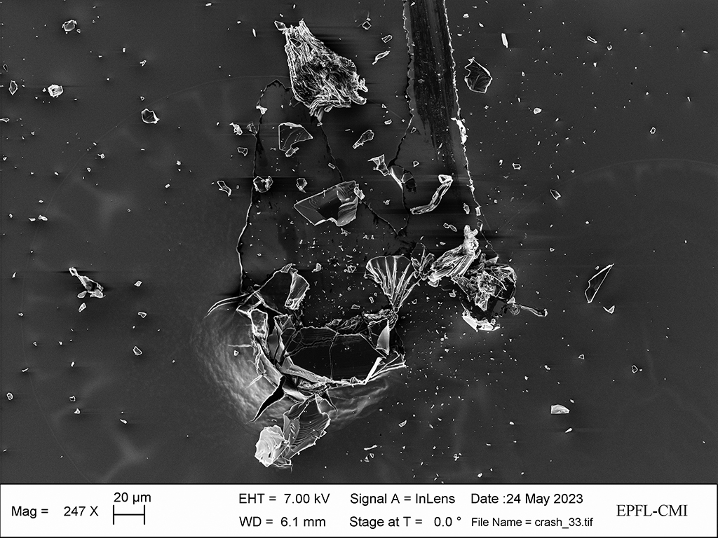
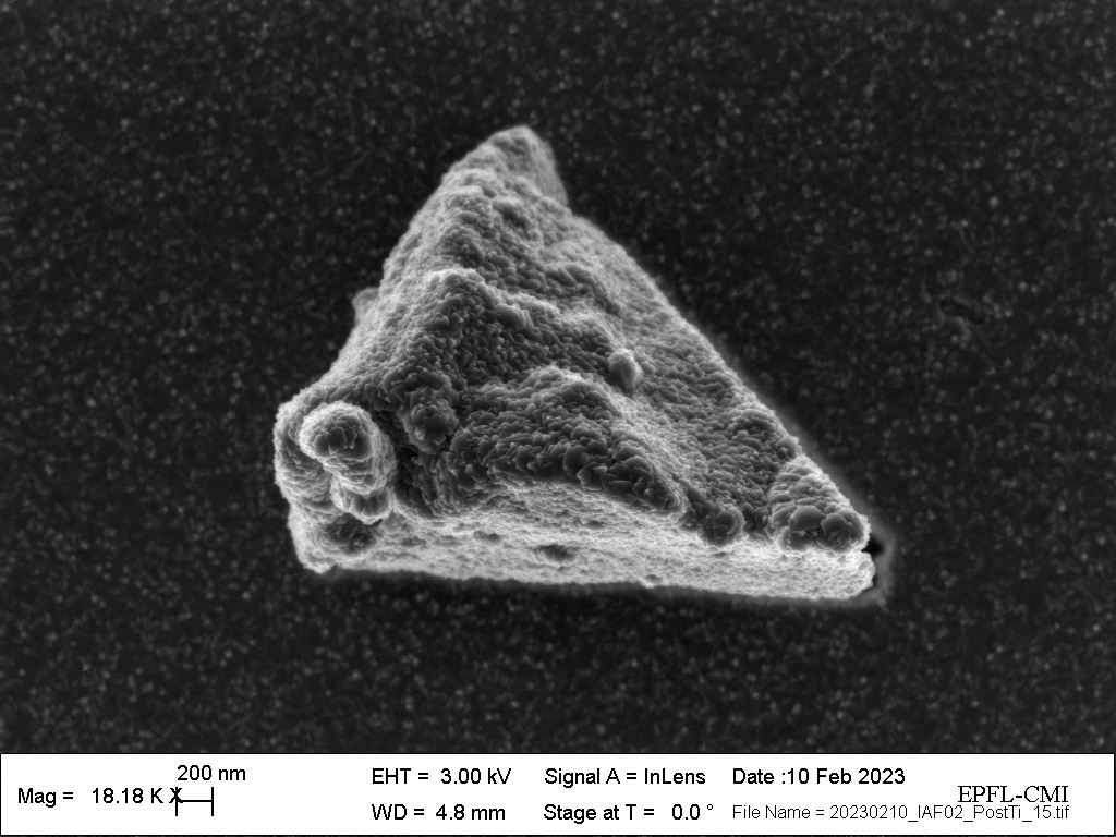
Crash_33
Philippine Milward, SQIL
Too harsh a landing on planet Silice! The boosters of the spaceship stopped working last minute, luckily, the whole crew escaped on time. To be a bit more serious, the corner of the chip cracked when trying to remove it from the carbon tape of the SEM sample holder creating some beautiful silicon impact on a layer of MMA/PMMA covered with aluminum.
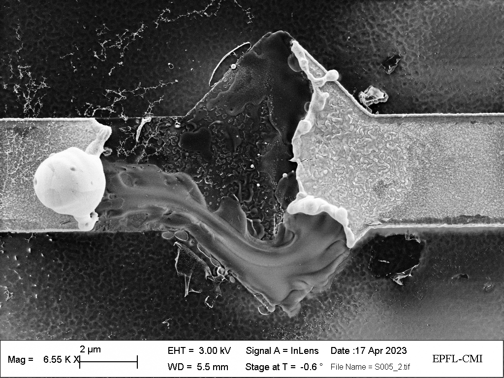
Lava_patch
Philippine Milward, SQIL
A volcano has erupted on my chip and disappeared just leaving a patch of melting lava! Hmmm, this might be an overdramatic interpretation. What happened is that some leftover resist interfered with the adhesion of aluminum on a silicon substrate. More accurate, but definitely not as cool as a micro-lava field.
2023, April
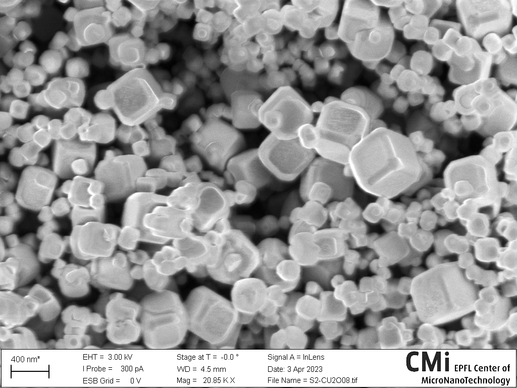
Stanley Cuprite
Elif Nur Dayi, LNET
Copper is a metal we all know, and as most metals it likes to reflect light. But when it oxidizes it turns into a semiconductor. One of its oxides which is seen here is called “Cuprite” and it loves to absorb light! These cuprite nanocubes are to be used as light absorbers and catalysts to convert sunlight to chemical energy. The “padding” on the cube corners is actually a sight for crystallography enthusiasts: They are the {110} facets while sides of the cube are {100}, and they react totally different as catalysts!
Iridium ice cream
Mohammad Rezaei, POWERlab
Plasma at nanometre scale is quite a mystery! Sometimes it produces a THz signal, sometime it makes a scoop of ice cream for you! Indeed, if you can digest Iridium.
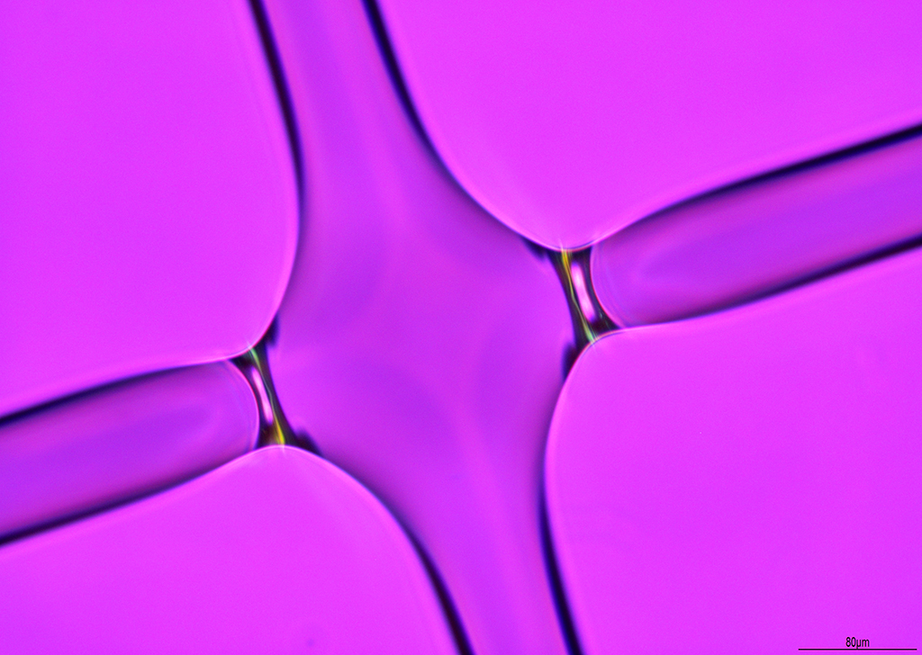
Vingt mille lieues sous les mers
Vittorio Bonino, HYLAB
Imagine voyaging deep in the ocean, where you may encounter mysterious creatures and breathtaking landscapes. But in this case, instead of water, you’re immersed in poly(3,4-ethylenedioxythiophene), a conductive organic polymer, and your submarine is a Leica DM800 optical microscope located in the CMI cleanroom. The creatures are iron(III) tosylate crystals and the bubbles on the border of the chip are residuals of solvent used for the polymerization of the PEDOT. Bon voyage!
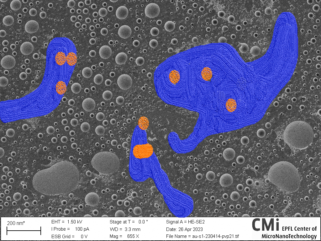
20000 Microns Under The Sea
Elif Nur Dayi, LNET
A moment of heated discussion between sea creatures, with the beam looming right above their heads. The bubbles are colloidal Au nanoparticles with sizes varying from ten to few hundred nanometers. They were dropcasted onto Si and will later play an important job as photocatalysts: converting light to fuels! However, some of them melted before their mission and morphed into these “sea creatures” during sample preparation and under beam exposure.
2023, March
Oxide Tree with Blue River and Snow
Silvan Stettler, NEMS
When venturing into the snowy Swiss Alps in winter, crossing rivers can be a dangerous endeavor. A recent storm of XeF2 has cut down a tree composed of SiO2 and Al, forming a narrow bridge to the other side. Cross it at your own risk, the water is shallow and falling into the spikey silicon riverbed would be painful!
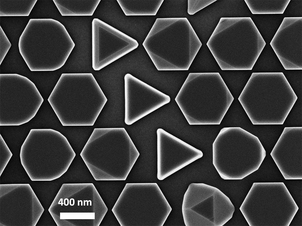
A triangle queue in the hexagon jungle
Michele Zendrini, LMSC
GaAs nanoplatelets grown by metal organic vapor phase epitaxy (MOVPE) after electron beam lithography of SiO2 mask for pattern definition. The originally patterned Y-shapes evolve into several morphologies during growth. Most of them resemble hexagons and polyhedrons, but some triangular specimens still struggle to survive!
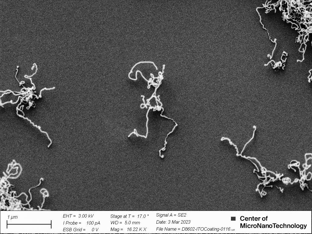
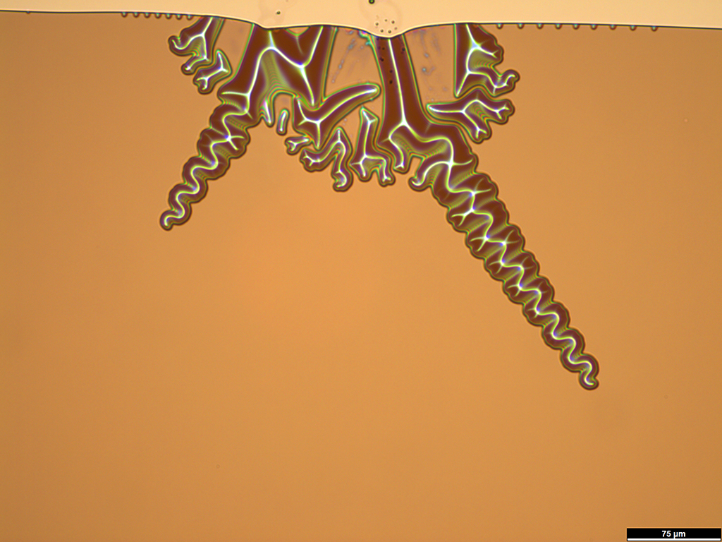
Dancing girl in the crowd
Zheru Qiu, LPQM
These nanowires are form inadvertently created after sputtering of ITO (in the SPIDER) on a SiO2 substrate with mysterious contamination. Although beautiful, I don’t want to see her again on my next sample. My current best guess is there was some photoresist or etch polymer remaining on the silicon oxide surface, which I didn’t expect. And it works as nucleation centers for the ITO and make it grows like nanowires.
Modern Line Art
Massume Zaki, NAM
This picture was supposed to be a golden gratings made using HSQ as a resist, but because of charging in IBE or due to HSQ not sticking well to the substrate, it became a black and white painting.
Micro-Joy-Waves
Önder Soydal, POWERlab
This is a SEM (Zeiss Merlin) photo of Ni/Pt metal stack deposited by EVA760 on GaN-on-SiC chip and patterned by E-Beam lithography (EBPG5000+). All fabrication steps and imaging were done in CMi. Intended structure was interdigitated metal fingers that are separated by few hundred nanometer gaps; however, due to dirty surface, metal fingers could not be constructed as sharp as intended and they embodied wavy patterns on themselves. How these amusing and malleable wave patterns came alive on rigid metallic structures is a great allusion to how life always finds its unique way to harmonize joy and seriousness in one body even during failures. As its nature, this structure also resembles CMi members who we fail to be distinguishable from each other behind the standard cold masks and gowns in the cleanroom, yet who have unique and joyful research ideas in their minds. Furthermore, the wavy patterns foreshadow the electromagnetic waves that would have traveled through these fingers if the fabrication was successful.
VO2 nucleation bacteria like network
Anna Varini, Nanolab
Different defects can be found on VO2 film grown with PLD. In this picture you can see one of them – bacteria like network.
Edward Scissorhands is finally happy!
Michele Zendrini, LMSC
GaAs nanopyramids grown by metal organic vapor phase epitaxy (MOVPE) after electron beam lithography of SiO2 mask for pattern definition. The shape of Edward Scissorhands results from lateral overgrowth of the pyramid structures that tend to merge as a thin film rather than remaining separated and well-defined.
2023, February
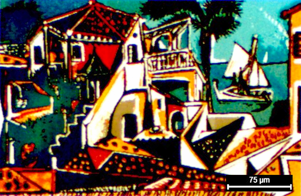
The day of the structural nanopainting
Hsiang-Chu Wang, NAM
This Mediterranean landscape is a combination of chromo-encryption and Picasso’s artwork observed under the optical microscope with polarized illumination and detection. Do you feel the breeze and the atmosphere of a nice weather in the summer?
The visualization of polarization-controlled chromo-encryption
Hsiang-Chu Wang, NAM
In this modern digital world, information that used to be recorded in binary format can now be encrypted in colors and decrypted only with a predefined numbering table and correct polarization pairs. There is a part of my thesis stored in this image! Does it not look like a random mosaic artwork?
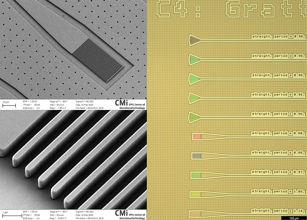
Colorful Brushes!
Zihan Li, Junyin Zhang, LPQM
Colorful Brushes! Grating couplers are fabricated on thin-film lithium niobate, to couple light from fiber into integrated cavities. Due to the interference in the visible spectrum, the grating couplers just look like colorful brushes in the optical microscope (right picture, directly exported from the optical microscope without further manipulation). The SEM picture for the grating are attached left.
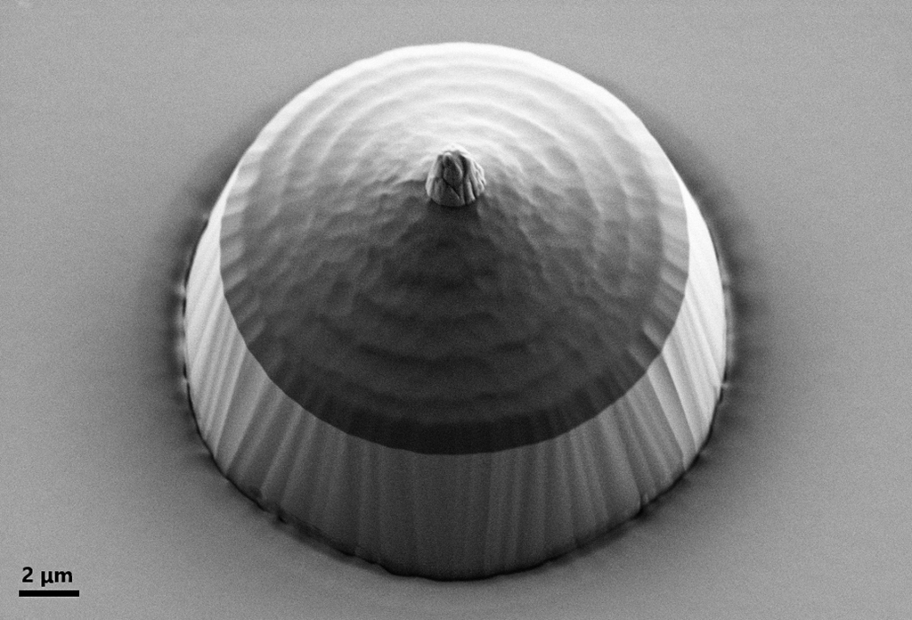
Micro-Yurt
Stefano Marinoni, LMSC
Looking for a micro-accommodation for your nanostructures? You can now rent a micro-yurt! Using two-photon grayscale lithography, this 20 μm-wide tent was etched into GaN, and shows a silicon dioxide roof to ensures optimal insulation against any weather condition. The picture was taken on the SEM Zeiss Leo.
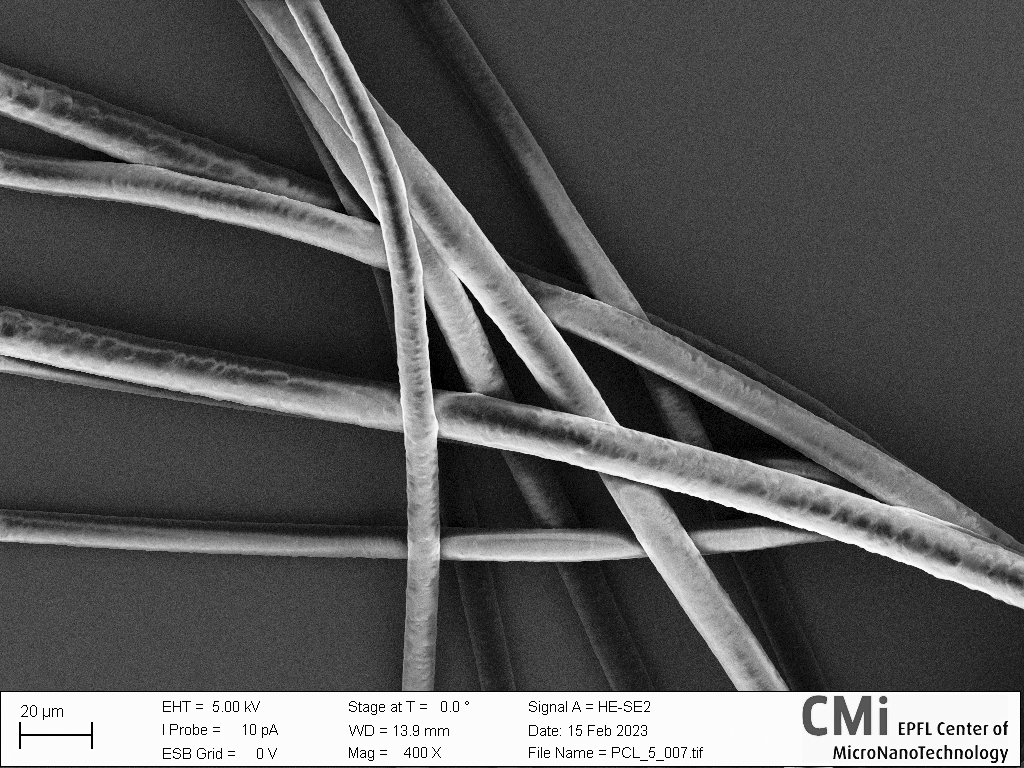
Highway interchange
Roberto Russo, Biranche Tandon, LMIS1
A micron highway interchange for cells and bacteria to crawl over and change their fate!! Poly-Capro Lactone fibers printed in multi-layer form weird cross over regions where a direction change in printing is carried out.
Diamond chewing gum
Yuchun Zhu, LQNO
This is a “diamond chewing gum” unintentionally made by me…
Crystal grape
Chengli Wang, Zihan Li, LPQM
A thin-film lithium niobate is bonded to the SiO2 substrate. But after dicing the wafer to small pieces, the lithium niobate film on the boundary begins to detach from the substrate and shrinks due to the stress. The wandering pattern looks like the mountains on the chip, or a bunch of grapes waiting for harvest.
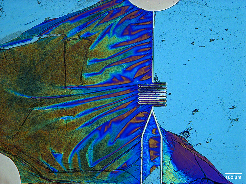
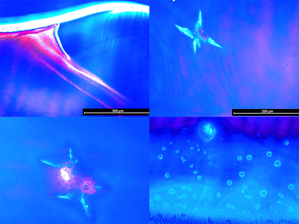
At the twilight’s crossing
Diego Armando Sandoval Salaiza, LAPD
In the picture there are SU-8 waveguide crossing constructs, showing birefringent behavior under polarized light microscopy. To further the story we’re still determining what is actually causing the birefringence, and it seems to be some particularities of the structure arising from the fabrication technique.
Galette des Rois
Claudio Jaramillo, LQNO
Inspired by the traditional “Galette des Rois”, we found out that the ovens at CMi can also bake micro-pies ! Starting with a single-crystal diamond substrate, deposit 200 nm of Titanium, and after baking at 200 °C for 45 mins (or until golden brown), out comes a Titanium-flavored pie. Serve while it’s hot, and enjoy with a cup of coffee.
2023, January
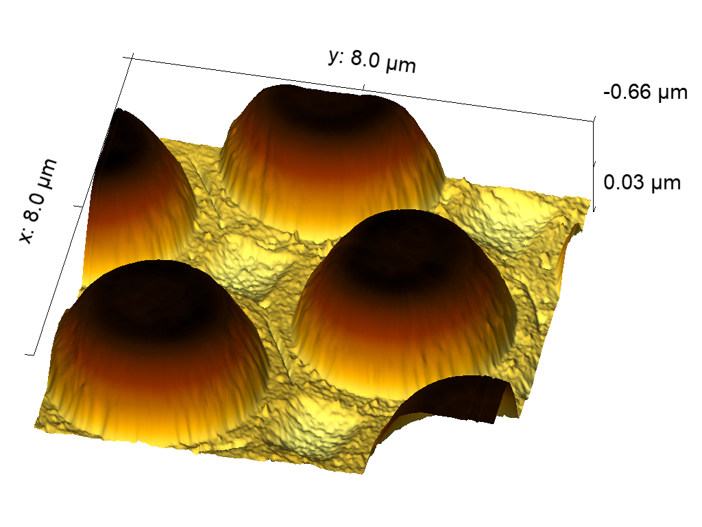
Nano Ayers Rocks
Roberto Russo, LMIS1
When you flip of 180° your boring dose test AFM picture ad you find out you were teleported in the middle of Australia! Overexposed IBE etched gold-coated superconducting YBaCuO sample.
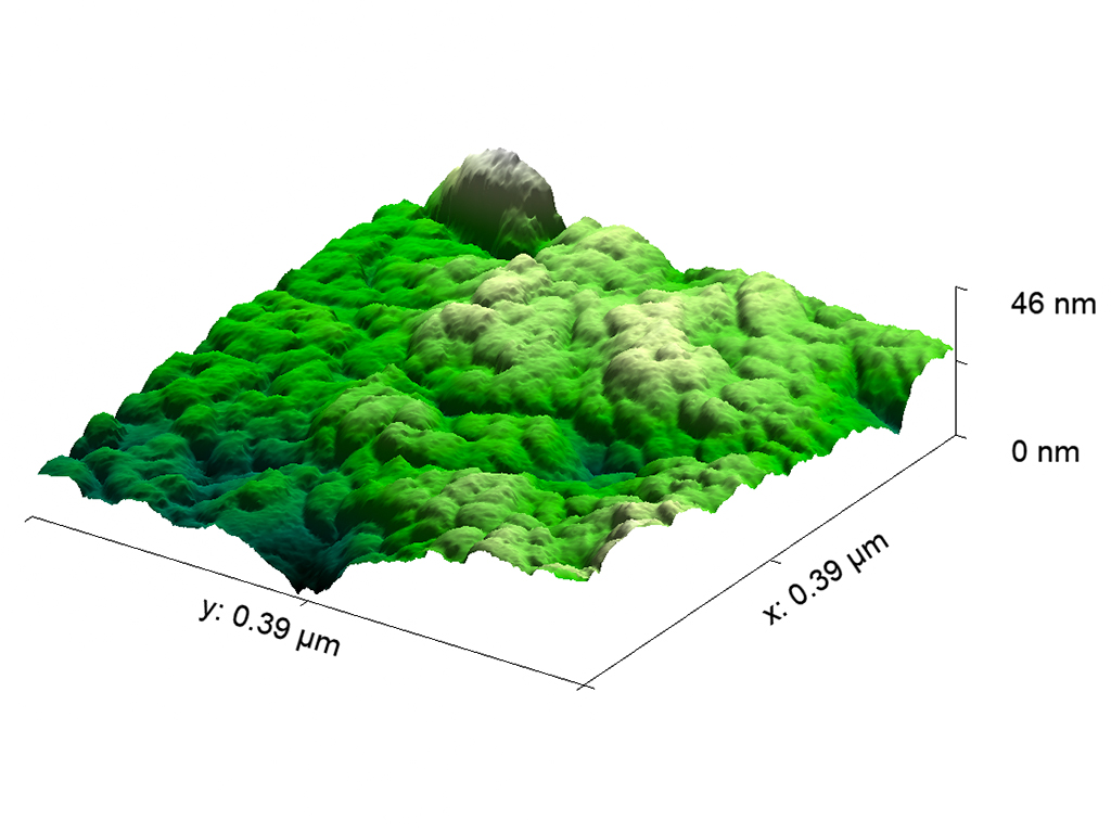
Nano Amazon Forest drone view
Roberto Russo, LMIS1
If you properly recolor an AFM scan, it can bring you anywhere! Here you can fly on drone wings over the top of Amazon forest. Surface grainy roughness of an IBE etched gold-coated superconducting YBaCuO sample.
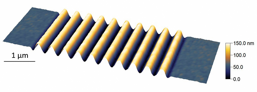
Not another earthquake
Berke Erbas, LMIS1
AFM image of sinusoidal pattern fabricated on thin film oxide by combining thermal scanning probe lithography and dry etching.
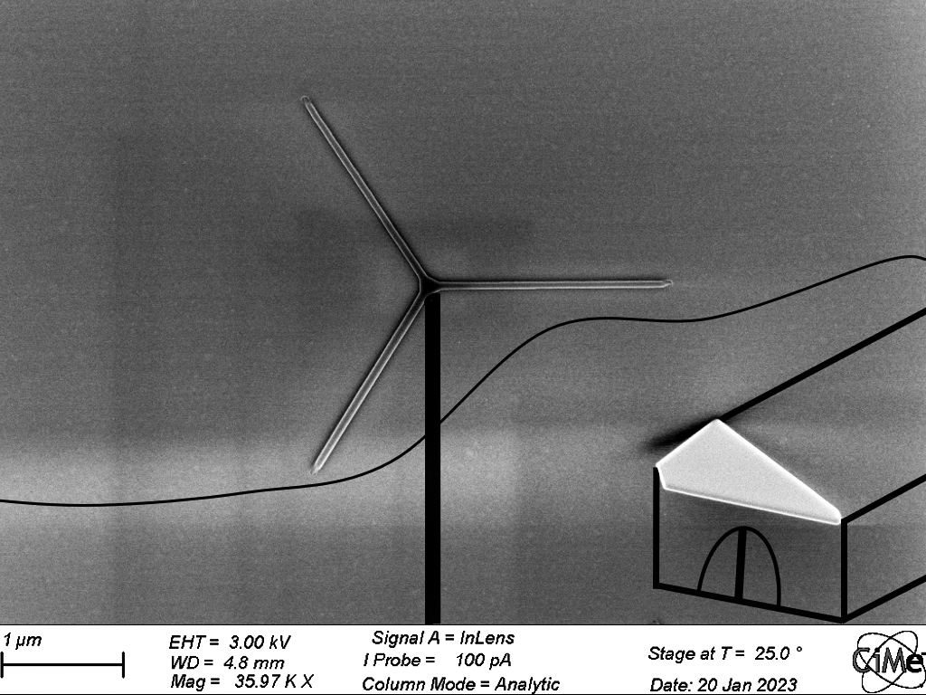
GaAs wind turbine in the SiO2 countryside
Michele Zendrini, LMSC
Branched GaAs horizontal nanowires grown by metal organic vapor phase epitaxy (MOVPE) after electron beam lithography of SiO2 mask for pattern definition. On the right side, at the top facet of the farmhouse, a randomly shaped parasitic structure grown on a defect of the mask.