Back to the current year Winners
2021, December
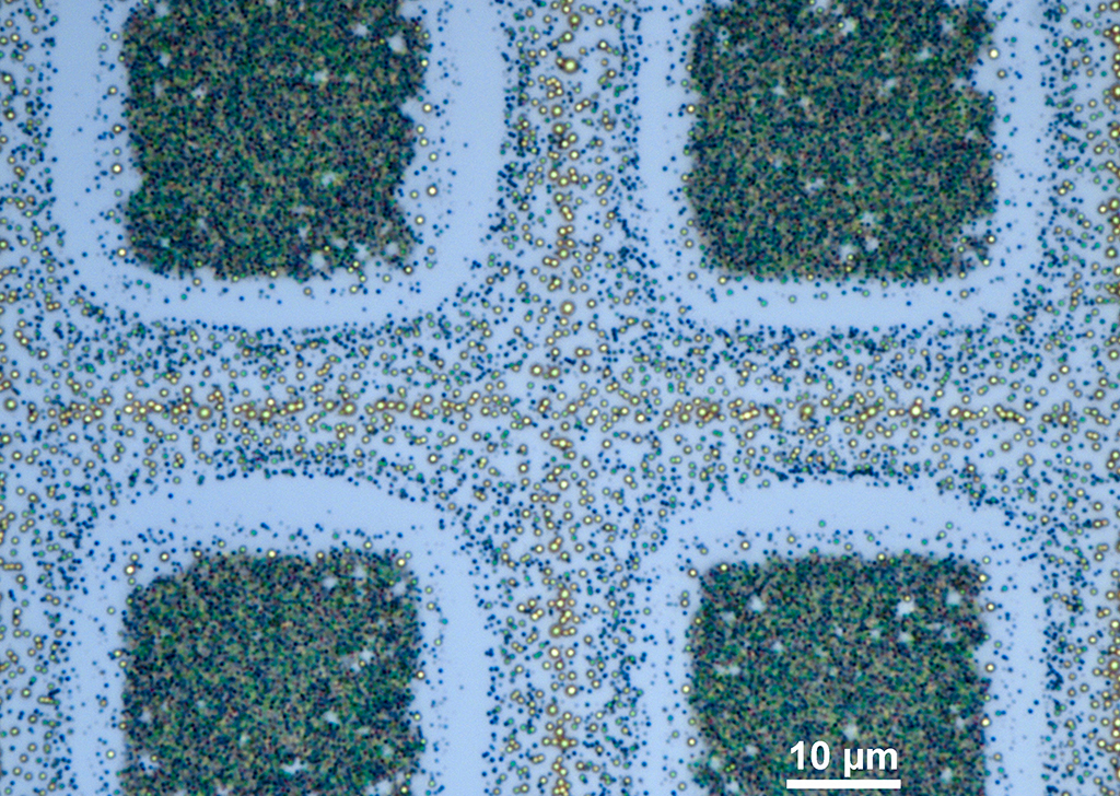
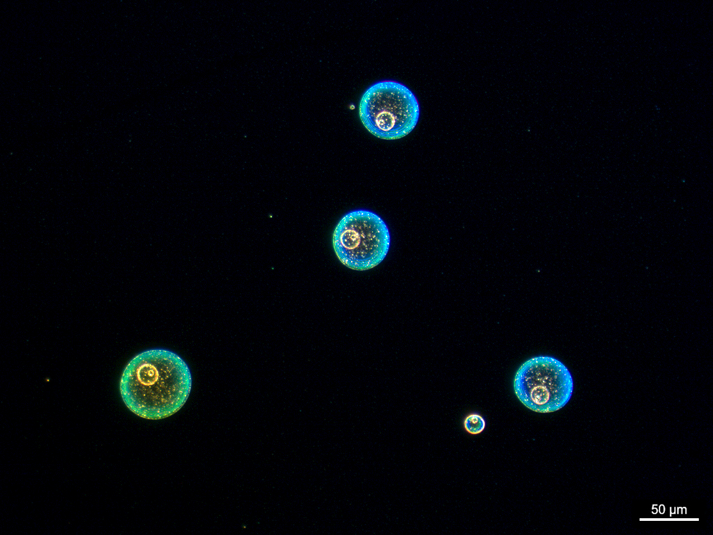
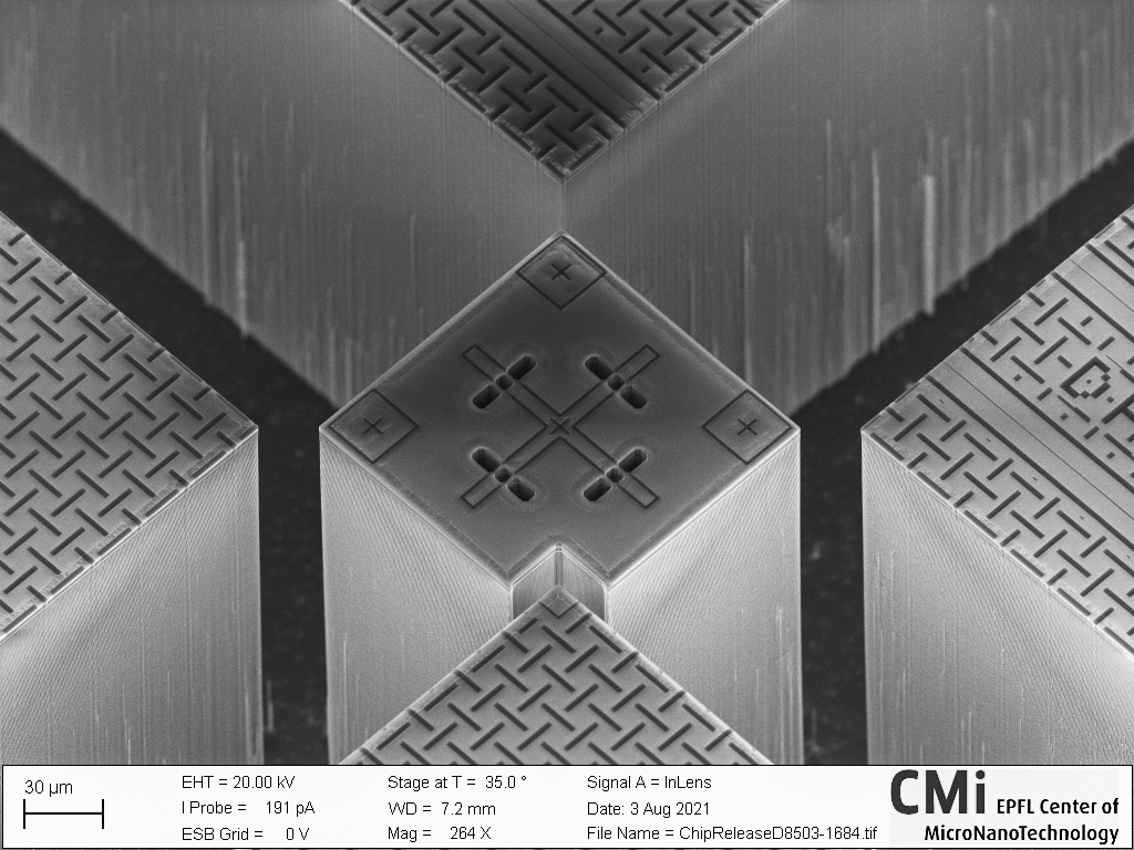
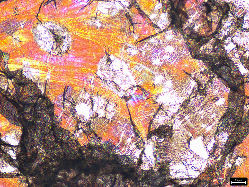
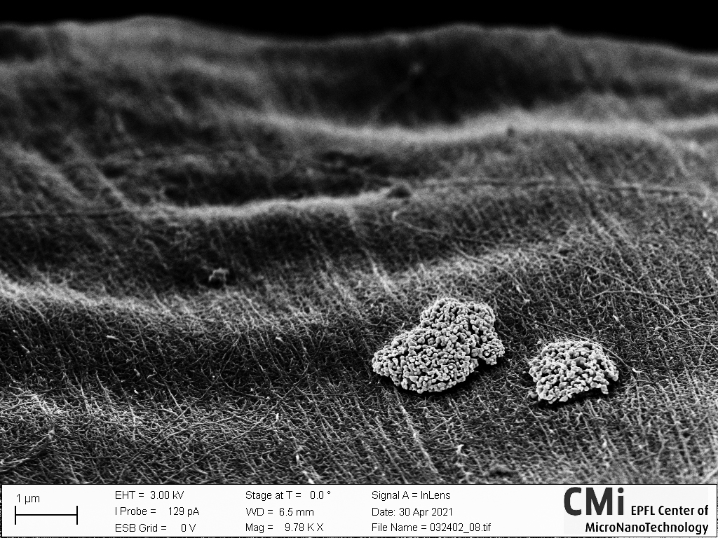
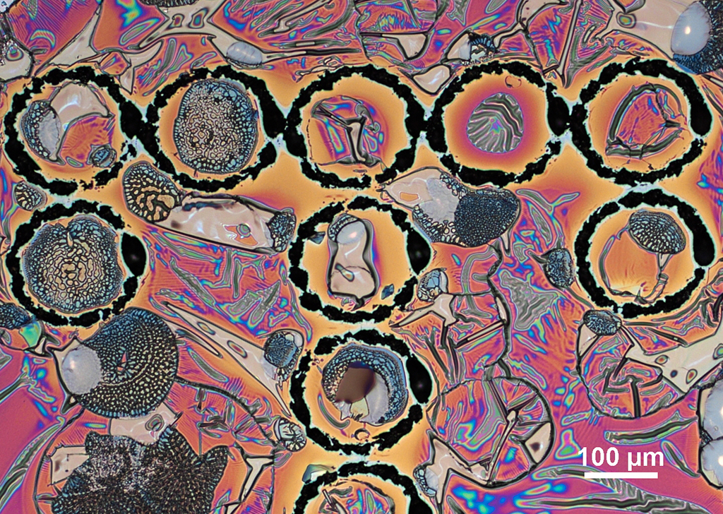
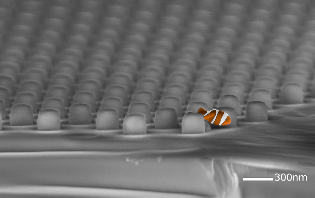
Beach of gold beads
Lorenz Hagelüken, LMIS1
This combination of symmetry, alignment and yet chaotic arrangement of green, blue and golden micro/nano particles results from 1000°C argon pyrolysis of some Nanoscribe 2PP structures printed on a silicon chip and coated with Parylene-C (Comelec) and gold (DP650).
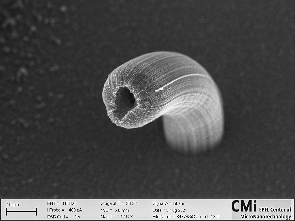
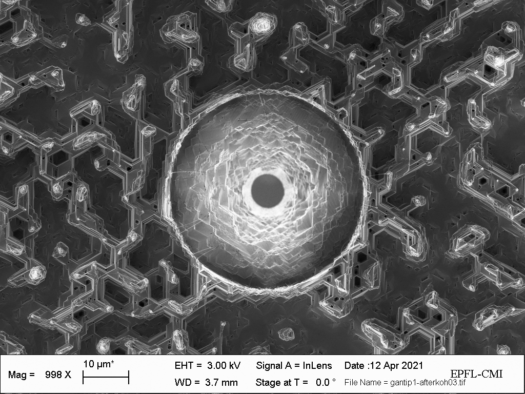
Secret of spiral pasta fabrication uncovered at CMi!
Daniel Moreno, NEMS
EPFL scientists have finally been able to reproduce one of the Italians’ best-kept secrets, the spiral pasta. Using the most advanced microfabrication techniques, Swiss people will now be able to switch from the boring späzli. The spiral pasta can be created when chlorine chemistry (in STS) finds holes in the photoresist and reacts with the underlying Aluminum. Just add tomato sauce and enjoy!
2021, November
Play Tetris in CMi
Jihye Lee, BIOS
The mesh metasurface, born with a heavy mission to become a quantum light-emitting device, became a Tetris game block that formed multimino (such as tetromino and pentomino) due to anomalies in the metal lift-off process after the e-beam lithography. Although this structure did not enter the quantum world, it will intrigue us in the CMi world. I learn today that the world of CMi is “Easy to learn, hard to master”.
Baby Fern
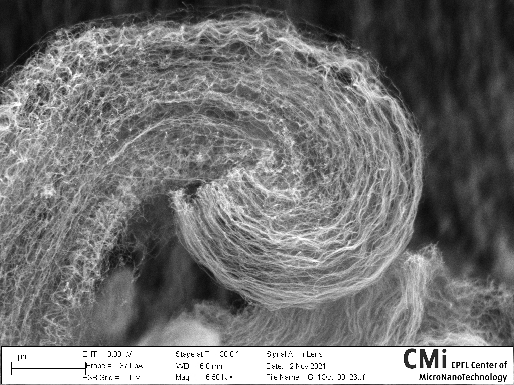
Hung-Wei Li, NANOLAB
After the deposition of metal, buffer layer, and catalyst in CMi, dense carbon nanotube forest grew on the substrate. We would like to observe the surface after measurement, and we found the baby ferns in the carbon nanotube forest!
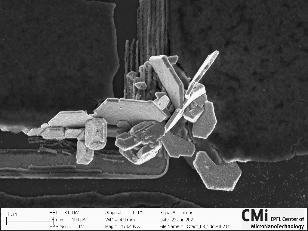
Alumina Ocean
Sylvain Mario El-Khoury, LMSC
In the depth of the Alumina Ocean, these strange jellyfish species can be found. Born from unexpected pinholes, they have been fossilized under hundreds of nanometers of silica, waiting to be discovered since then.

Winter flower
Elena Losero, LQNO
Winter is coming, but this not polished CVD diamond chip presents several overgrown crystals, which remind flowers in a spring garden.
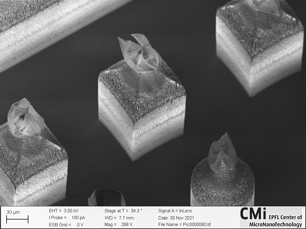
Silicon-based Pastry
Ali Gilani, NANOLAB
The curious mind is sweetened by looking at these solid silicon-based microneedles resembling pastry. The cherry on the cake is a silicon-oxide mask thinned during the fabrication process.
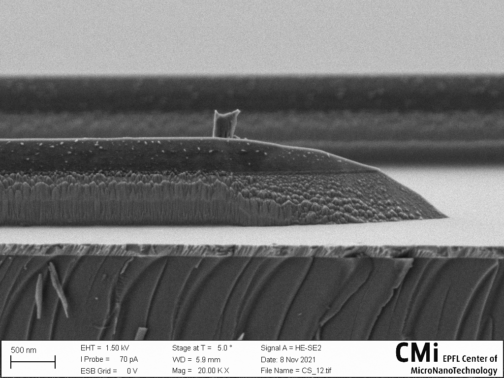
Bullet train
Zihan Li, LPQM
The SEM of the end of our waveguides fabricated by the mentioned process flow: deposit hard mask on lithium niobate wafer, and expose by a stepper in Zone5. The pattern is some lines or rings (waveguides and resonators). After development and IBE etching, they look similar to the train.
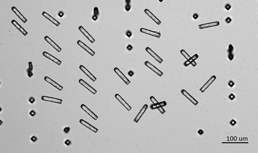
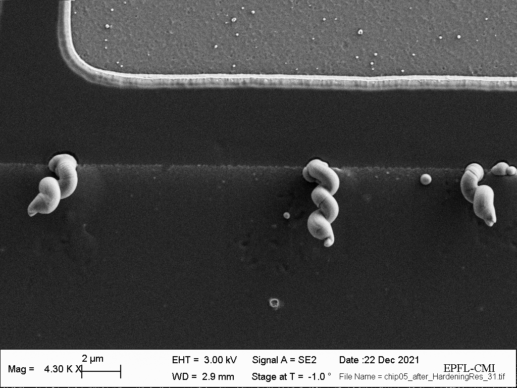
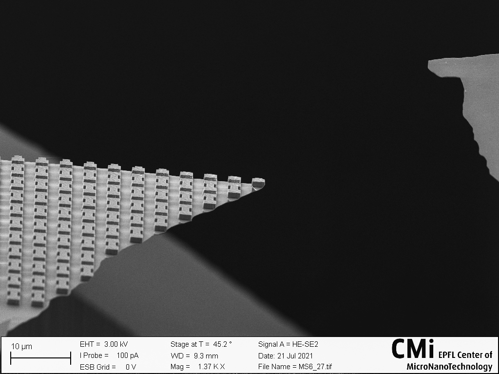
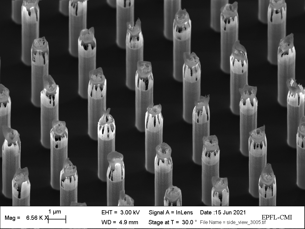
Cutdown forest
Raphael Dezauzier, LMIS4, ArcoScreen
A forest was cut down this month by the CMi lumberjacks, as can be seen by the look of these logs! When growing polymer micropillars using a 3D laser writer, they tend to detach from the glass surface later on during the washing of the remaining resin. This is due to the tremendous capillary forces present during the evaporation of the development solvent.
2021, October
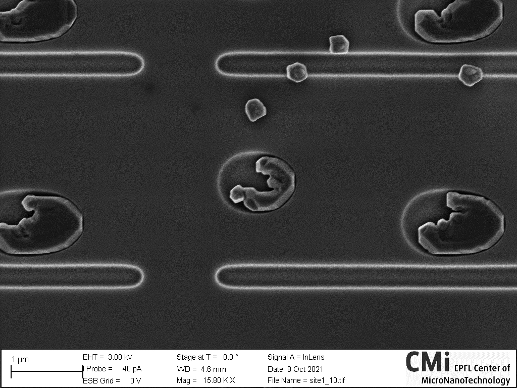
Germanium Embryos
Antonia Gundel Hager, LMSC
These Germanium-Embryos are embedded in their wombs in an oxide mask, originating from air enclosures in a thin PMMA layer. The embryos are nourished by metal-organic precursors so that they can grow to their best crystal liveliness.
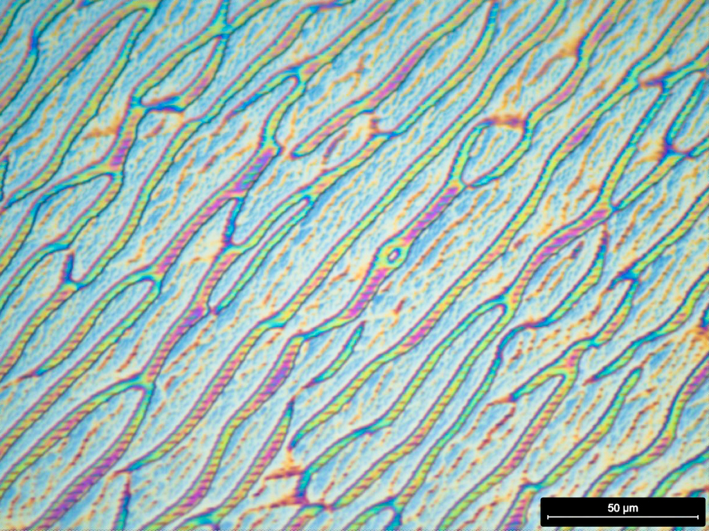
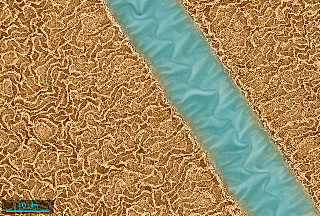
PDMS Wallpaper
Antonia Gundel Hager, LMSC
These colorful patterns could be a wallpaper design – but in fact it is interference at its best, after a nanopatterned PDMS-stamp was squeezed all over the place on a resist layer.
2021, September
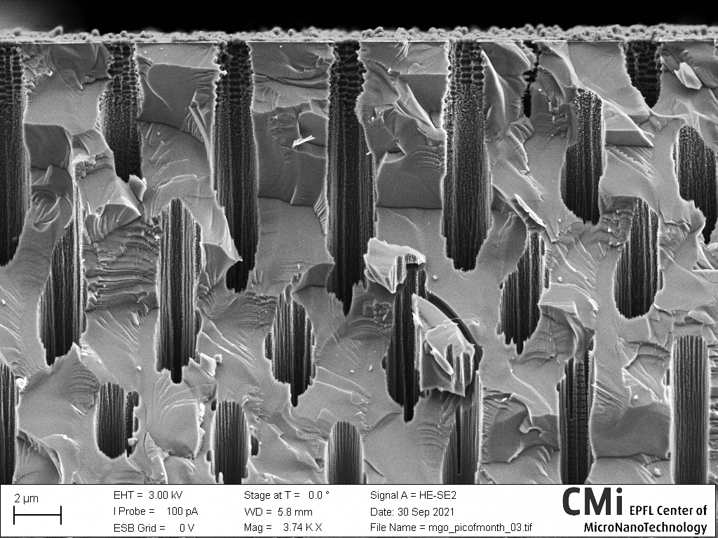
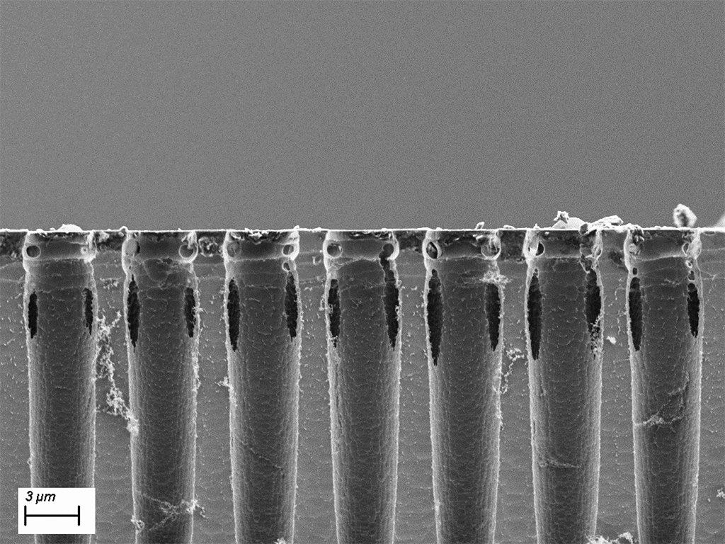
Silicon waterfalls!
Mohammad Beygi,
Samira Frey, PV-LAB
High aspect ratio channels etched through 50 um thick amorphous silicon layer which is deposited on top a silicon wafer.
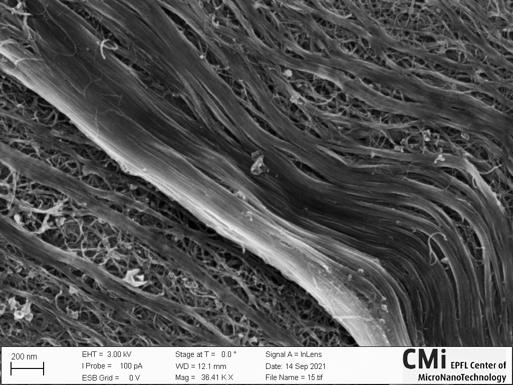
Carbon nanotubes falls
Pierrick Clément, LMIS1
A new attraction has opened in CMi for the pleasure of all the users. While Niagara falls are the biggest in North of America, these carbon nanotubes falls are the smallest of the world! A tour in nanoboat will soon be organized to have a closer view.
2021, August
Helicopter field on top of a skyscraper
Zheru Qiu, LPQM
It’s a microscopic helicopter field on top of a skyscraper with fancy markers waiting for the next landing. No, sorry, it’s an alignment marker separated during deep Si etching to separate the photonics chips fabricated.
Garden eel
Hung-Wei Li, Nanolab
While diving in a tropical ocean, you may come across what appears to be a bed of seagrass gently moving with the current. But look more closely, you may spot garden eels! However, they are shy, and they will dig into the seabed immediately. The sample was fabricated in CMi and grow carbon nanotube (CNT) via our CVD system.
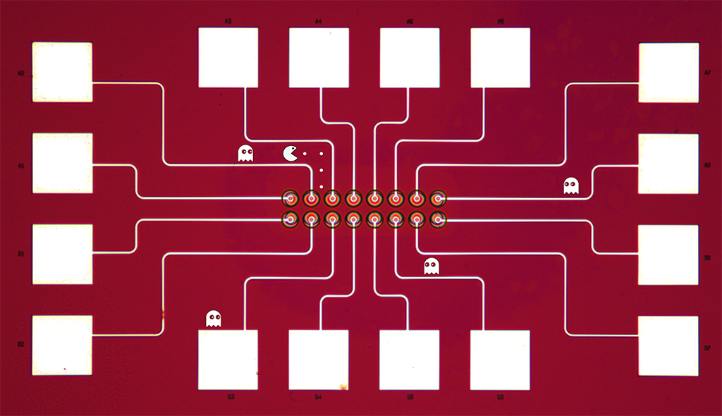
Steel Sliding Door to Enter the Escape Room
Jason Ruan, ADEPT Neuro SA
Did you hear that there’s an escape room at CMi-EPFL? No? Well, look at its entrance right here, it is the steel sliding door to start the game. I hope you will not stay trapped in CMi. The picture shows a bottom view of a smart chip, ASIC stands for Application Specific Integrated Circuit, intended to be integrated with deep brain electrode implants. The deep brain electrodes that will receive these magnificent smart chips are manufactured at CMi-EPFL.
2021, July
Artificial intestinal tissues are full of colours
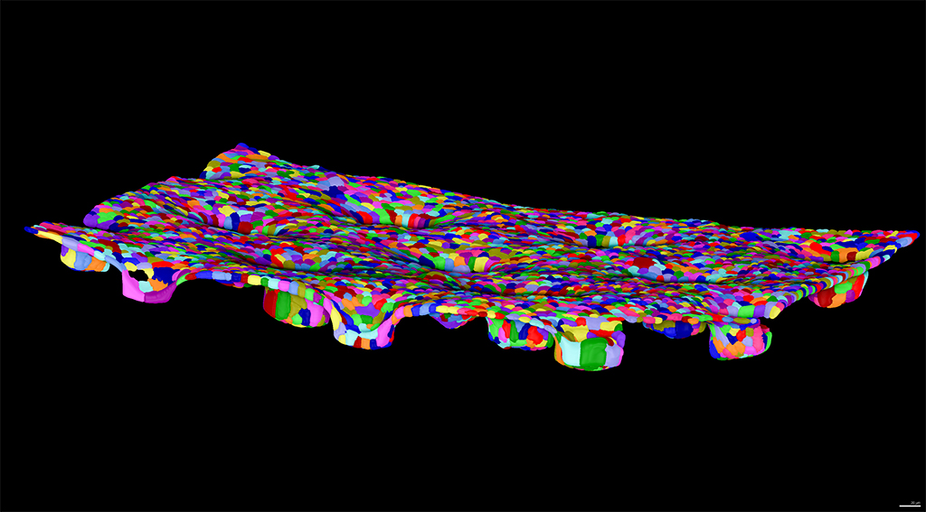
Moritz Hofer, LSCB
Intestinal tissues are composed of an epithelial monolayer with invaginations (“crypts”) that harbour the stem cells. Using microfabricated PDMS stamps we recreated hydrogel scaffolds on which we could recreate artificial intestinal epithelia with geometries akin to the ones of native tissues. Moulds for stamps were created using Si wafer dry etching. You look at a 3D visualisation of such in vitro cell monolayer, that was generated using confocal images of the cells’ fluorescently labelled membranes. Scalebar, 20um.
Michel-ANGLE-o
Felix Ulrich Richter, BIOS
These lucky silicon bricks are sitting at the edge of a bonded alumina membrane stretching out to touch its lost half.

Rising Sun
Roberto Russo, LMIS1
The sun is rising in CMI today! NbTi resonator on top of sapphire substrate.
2021, June
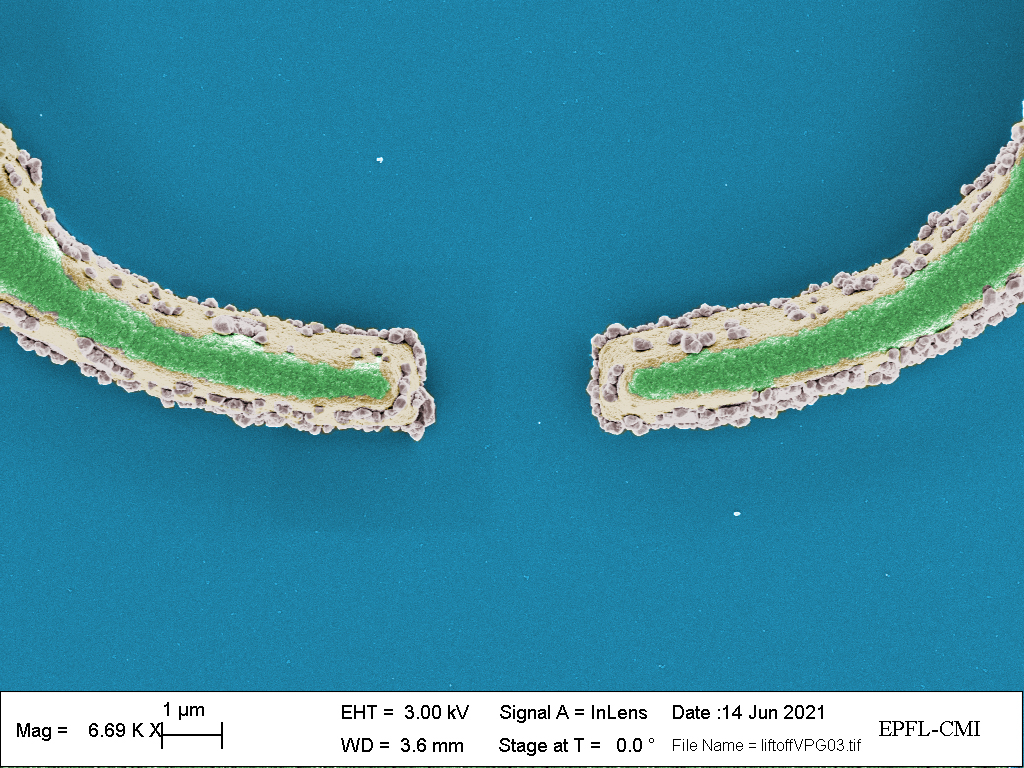
Harbor on a NbTi sea
Loïc Adrien Broyer, LMIS1
In ancient times, data transfer occurred by mail and ships, nowadays it is by email and chips. But an incomplete lift-off process has accidentally lithographed a harbor on a NbTi sea.
Board CMi!
Antonia Gundel Hager, LMSC
Are those the sails of a fleet of wild pirates on the horizon, sailing towards the sunset? If the anti-sticking chemical on a Nanoimprint Stamp doesn’t work properly and resist gets ripped off from the sample here and there, it’s a pity for the imprint but a win for your imagination.
Back into life
Antonia Gundel Hager, LMSC
These Algae made of Nanoimprint resist flowing around during an imprint process wait patiently at the seashore for the next waves to flush them back into the ocean. If only the weather doesn’t stay too calm…
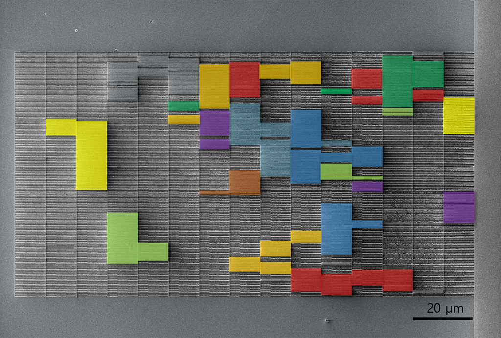
A concert of the Fab Four
Mohammad Bereyhi, Alberto Beccari, LPQM
A quartet of nanomechanical resonators fabricated at CMi from 20nm LPCVD silicon nitride on silicon wafers. From left to right: binary trees, stress-engineered nanobeams, polygon resonators, and phononic crystal nanomembrane all in one frame forming an ultra coherent string and drum quartet. Be ready for a long movement, because some of these instruments take up to four hours to decay if excited!
Be careful, smokers spotted at CMi!
Vincenzo Messina, ANEMS
These silicon butts are obtained after an etching attempt. The process should have resulted in still intact cigarettes, but apparently someone has a bad habit, and lit them before taking the picture.
Futuristic micro-building
Francesco Bertot, Q-lab
Who said that contaminations are always a bad thing? This time, observing the result of a Lift-off process after the bath in the remover, a contamination stuck on the surface presented this peculiar structure with concatenated hexagons. Could it become the project of a futuristic architect?
2021, May
Hibernating Bees
Samira Frey, PV-Lab
During the fabrication of funnel-shaped microchannels, we found these adorable bees inside the channels that appear to be still in hibernation. The main channels were etched using the Bosch process and a chromium hard mask. Afterward, an isotropic etching step was done to widen the top of the channels.
The spirit of Claude Monet in CMi
Pierrick Clement, LMIS1
It is commonly said that artists never die and a new frame, most probably from Claude Monet, has been reveled at CMi. He has used AZ1512 as photoresist to pattern a parylene layer and he anticipated that it would result in a bad stripping at the end of the process and generate these lovely sunset colors. This piece of art will be open to auction sale soon.
2021, April
Micromasking/Micromazing
Nicolas Tappy, LMSC
While deep-etching (sentech) nanoscribe prints in GaN, an oxide layer re-deposited on the substrate. KOH treatment did not improve the situation, but revealed this hexagonal maze of GaN m-planes, protecting the pyramid from intruders. Maybe a modern Daedalus would use it to imprison a micro-Minotaur?
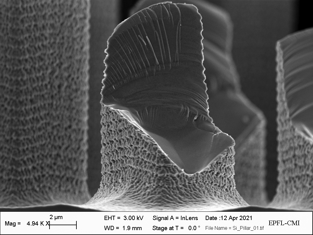
Who will conquer the Silicon Throne?
Xiaokang LI, Yen-Cheng Liu, Department of Oncology UNIL CHUV, BIOS
The Iron Throne has been destroyed thanks to a hot breath of the dragon, but the Silicon Throne is still waiting for its conqueror. This throne is created by accidentally cleaving a silicon micropillar, where the glow on the edges indicates a thin layer of dry oxide (Centrotherm furnaces).
Sea storm on our wafer
Hernan Furci, André Chatel, Loïc Adrien Broyer, LMIS1
Aerial view of an unchained silicon sea sending violent, turbulent, foamy waves onto a NbTi beach. Ion beam etching of NbTi on silicon (with undesired features on the etched regions).
Accompany me
Hung-Wei Li, Nanolab
After the deposition of metal, buffer layer, and catalyst in the CMi, a dense carbon nanotube forest grew on the substrate. There are salts deposited on the CNTs surface during the measurement. When observing the carbon nanotubes’ side, those salts look like two small creatures accompanying each other on the CNTs.
Coronavirus-EPFL-CMi-variant
Fatemeh Qaderi, Nanolab
The sample included pulsed laser deposited VO2 film on top of Tungsten. But this exact spot on the wafer is definitely something else. It could be some residue from the resist, or even a single virus just inhabiting on the wafer, the CMi-variant.
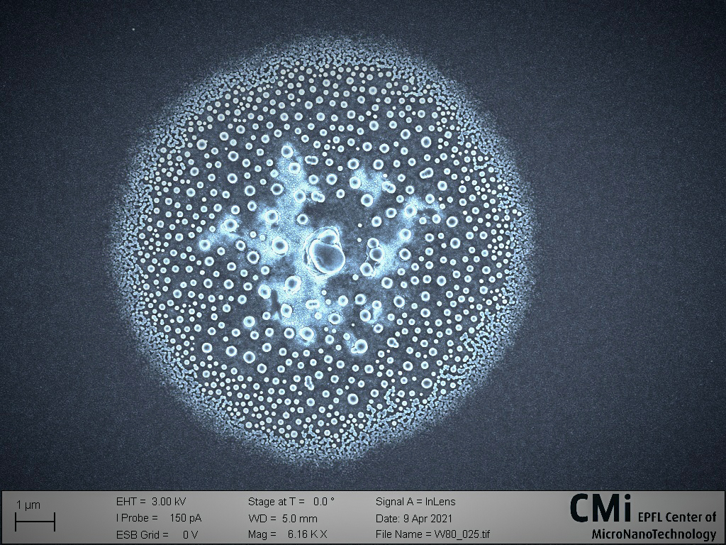
Go get those photons!
Andrea Giunto, LMSC
The figure shows PAC-MAN hurrying in a maze of GeSn single photons avalanche detectors (SPADs) fabricated on a Si wafer. Will PAC-MAN manage to recover all the IR photons before they are detected by the SPADs, or swallowed in the oblivion of the ghost (aka dark) counts? The magenta color is given by the SiN PECVD anti-reflection coating. Evaporation, sputtering, IBE, Ebeam lithography all contributed to the fabrication of the SPAD maze.
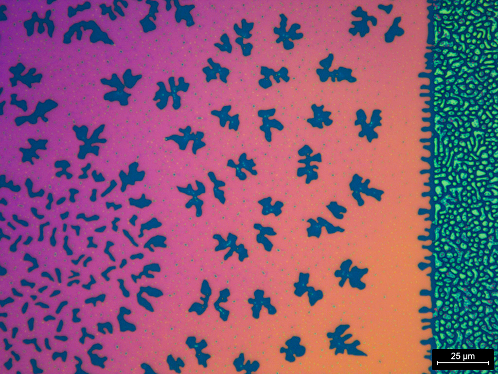
2021, March
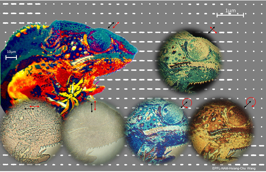
Structural color chameleon
Hsiang-Chu Wang, NAM
Structural color printing of a chameleon composed of Ag rods with different lengths aligned horizontally. The background shows SEM image of the nanostructures (sizes between 60 and 200 nm). The colors vary with the illumination (black arrows) and measurement (red arrows) polarization states. Muted colors are generated when both polarizations are horizontal or vertical. On the contrary, illumination along the diagonal directions produces exceptionally vivid colors, that stem from the dichroism of the structure. Only the correct polarization combination reveals these catchy colors in the optical microscope.
Broken Glass Art
Berke Erbas, LMIS1
SiO2 sputtering on resist coated substrate surprisingly led an art made by broken micro-pieces of glass. Ring, face, fingerprint, brain and dolphin shapes are created by randomness of the process rather than smooth coverage of glass on the surface.
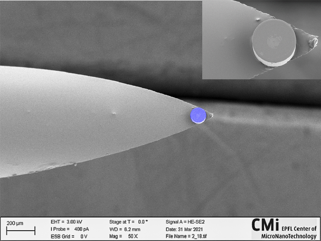
A microscale SU-8 at the tip of a needle
Zhiwei Yang, LMIS1
Do you know how to precisely place/transfer a microscale object at the tip of a tiny needle? Our answer is: using laser-induced forward transfer (LIFT) technique. Our LIFT setup enables the transfer of such object/structure to many non-planar receivers such as curvilinear surface and surface with prepatterned structures, which might be challenging for other transfer techniques.
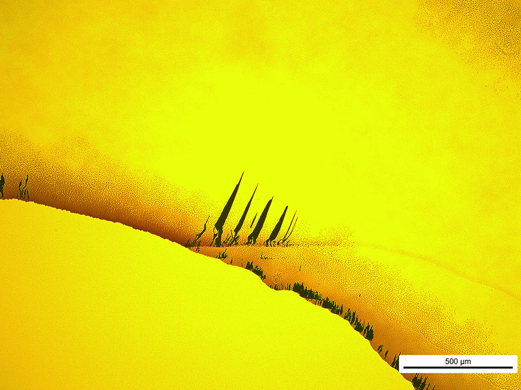
2021, February
Suez Canal
Matthias Neuenschwander, LBNI
The Suez Canal in Egypt was finished in 1869, connecting the Mediterranean Sea to the Red Sea. This micro version was inadvertently created at the CMi in 2021, when I tried to dry-etch a rectangular window into a silicon nitride film. As I was using a very fragile wafer, I had to attach it to a dummy using QuickStick. The cooling turned out to be insufficient and the resist overheated, creating the wrinkled structure. False-colored in Photoshop.
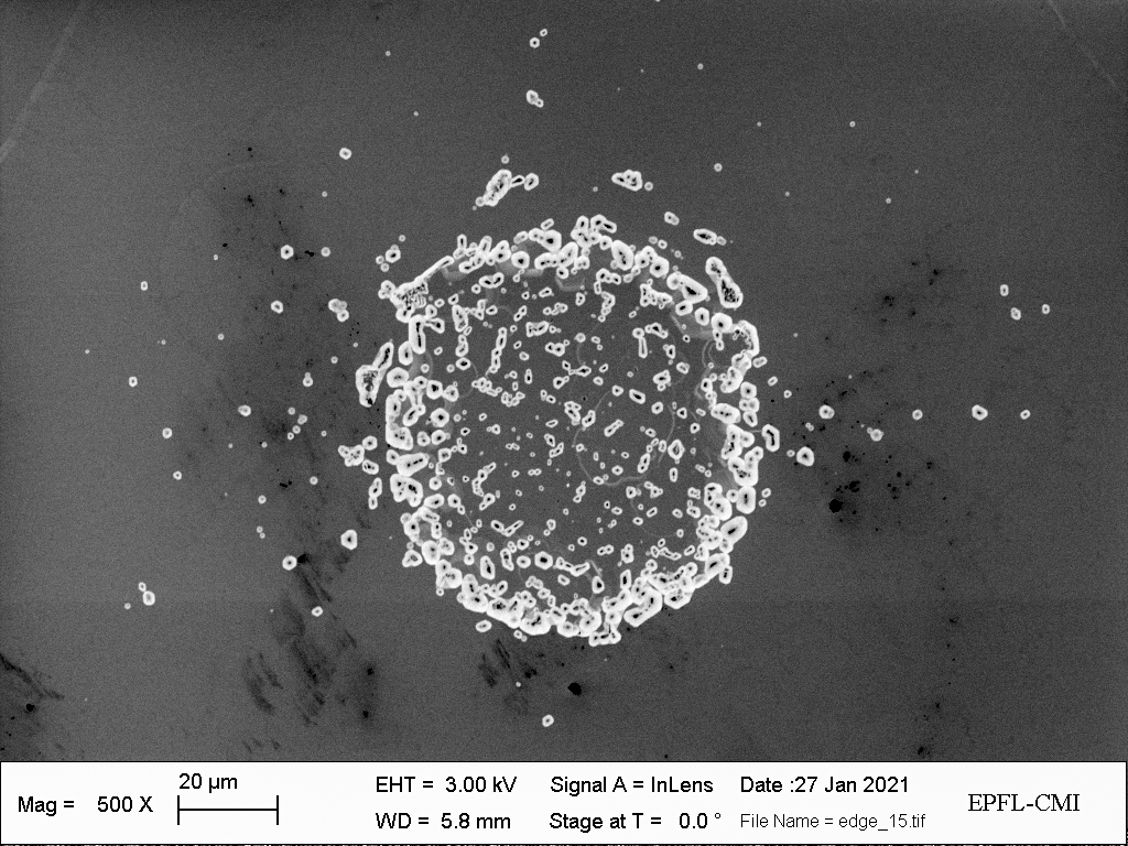
Nano CMi Galaxy
Pooya Dehghan, NanoLab
These nano-structures are made up of Carbon Nano Tubes(CNTs).
A Shy Little Inhabitant
Lucas Güniat, LMSC
While we were swimming around the oxidized phase-shift lithography Silicon nanopillar’s great reef, in order to asses their size expansion by oxygen incorporation, a little friend came and say hi timidly from afar. Certainly a by-product of dicing, it stayed quiet without moving when we passed in front of him. We managed to take a picture before continuing our journey.
2021, January
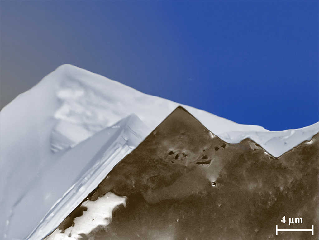
Sunrise over an 8000nm peak at CMi
Giovanni Resta, GAP–UNIGE
Summit day push on this tiny snowcapped mountain at CMi. A small tribute to celebrate the historic first winter ascent of K2 on January 16th 2021 from a group of 10 Nepali mountaineers. This a re-colored image of the edge of a silicon chip that has been cleaved by hand, leaving atomically sharp edges as well as more blunt features. Picture captured with SEM Merlin In-lens detector at 3KeV EHT.
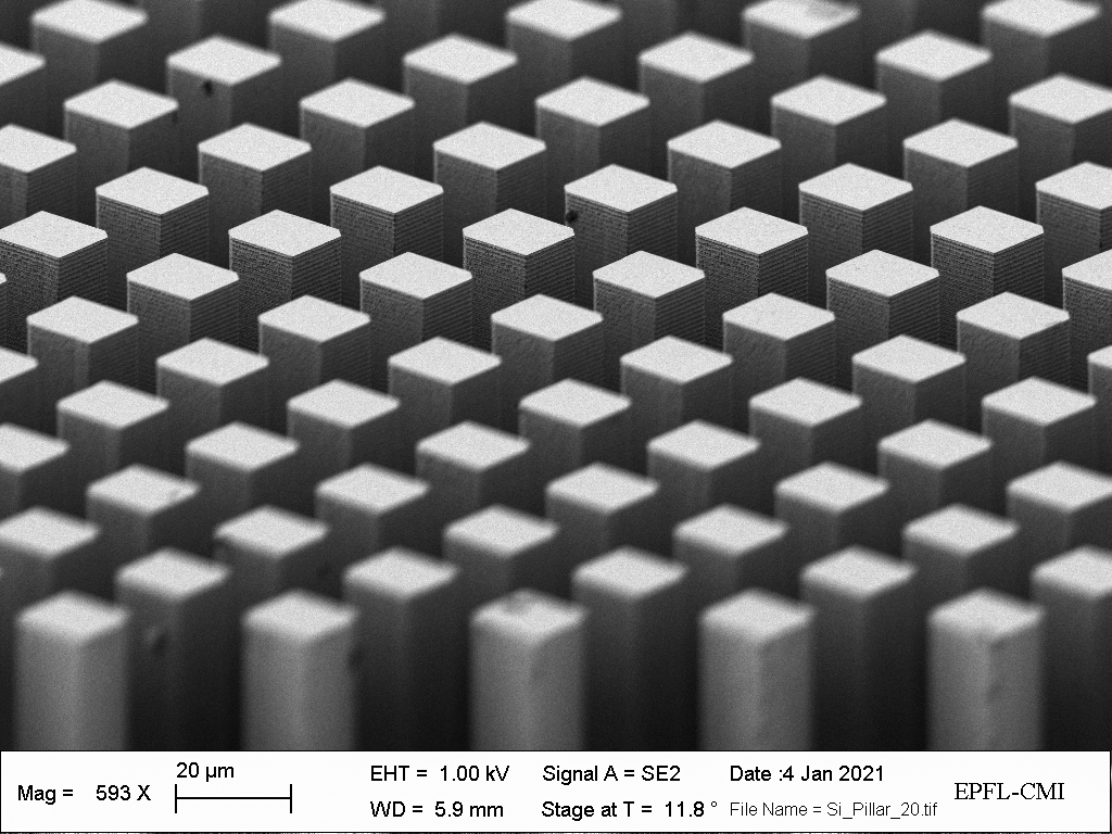
The city in 2263
Xiaokang Li, Department of Oncology UNIL CHUV
These silicon pillar arrays could represent the future look of our cities if the global population keeps growing. Without enough space to live, we would need to build higher and higher buildings that look like each other. What a boring world! Let’s act now to lead a sustainable life.
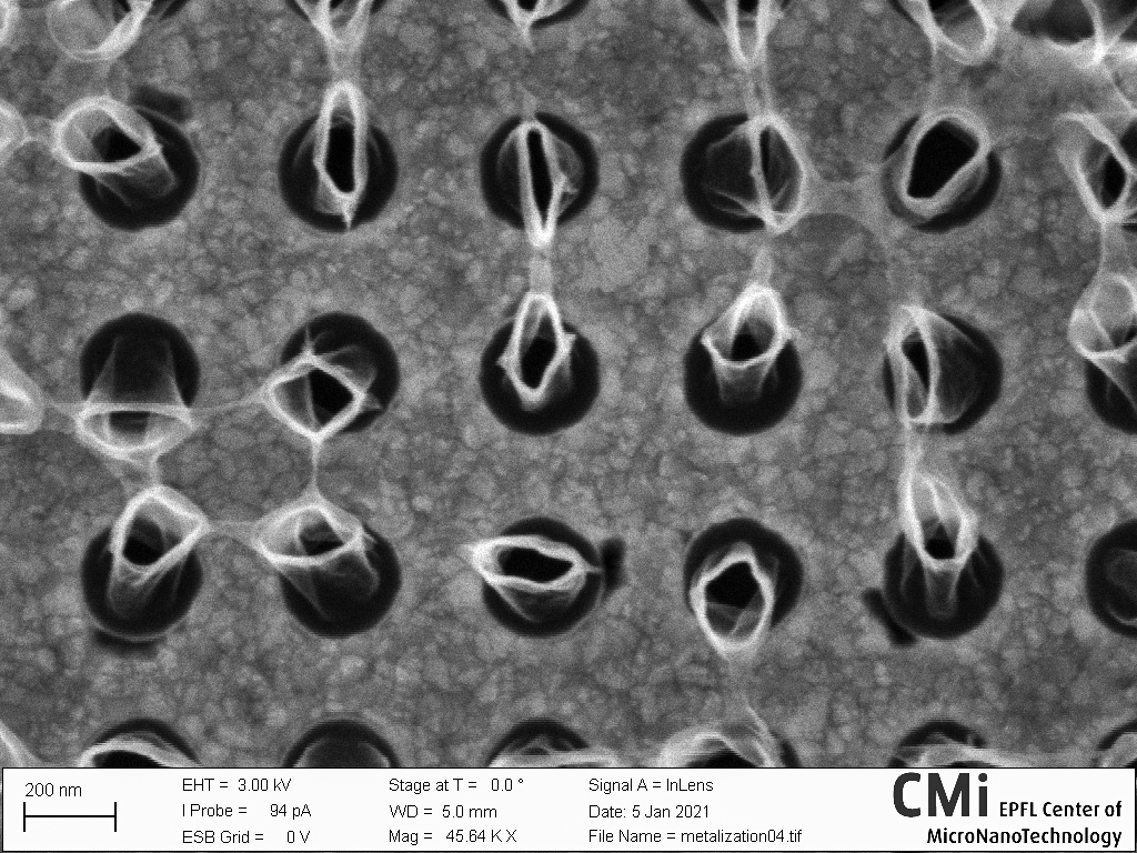
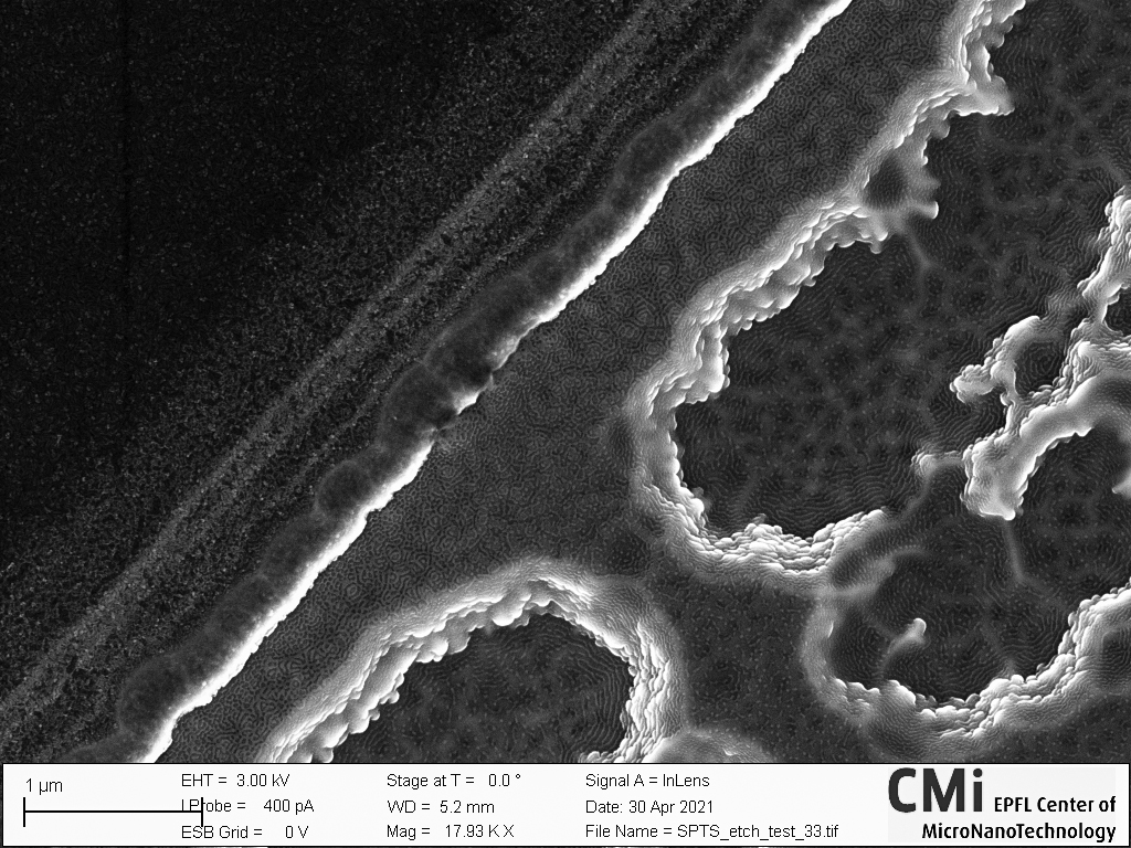
Dancing ghosts
Anna Varini, Q-Lab
When things don’t go exactly as planned at CMi you might unexpectedly find a cheerfully dancing ghosts that hold hands like in “Dance” by H.Matisse right where your real structures are supposed to be. Performance took place on Si wafer with multiple layers after final STS chlorine etch through 100nm Al layer. The origin of the ghosts is not exactly known, however, most likely results from underlying SiO layer and/or polymer formed due to passivation during chlorine etch.
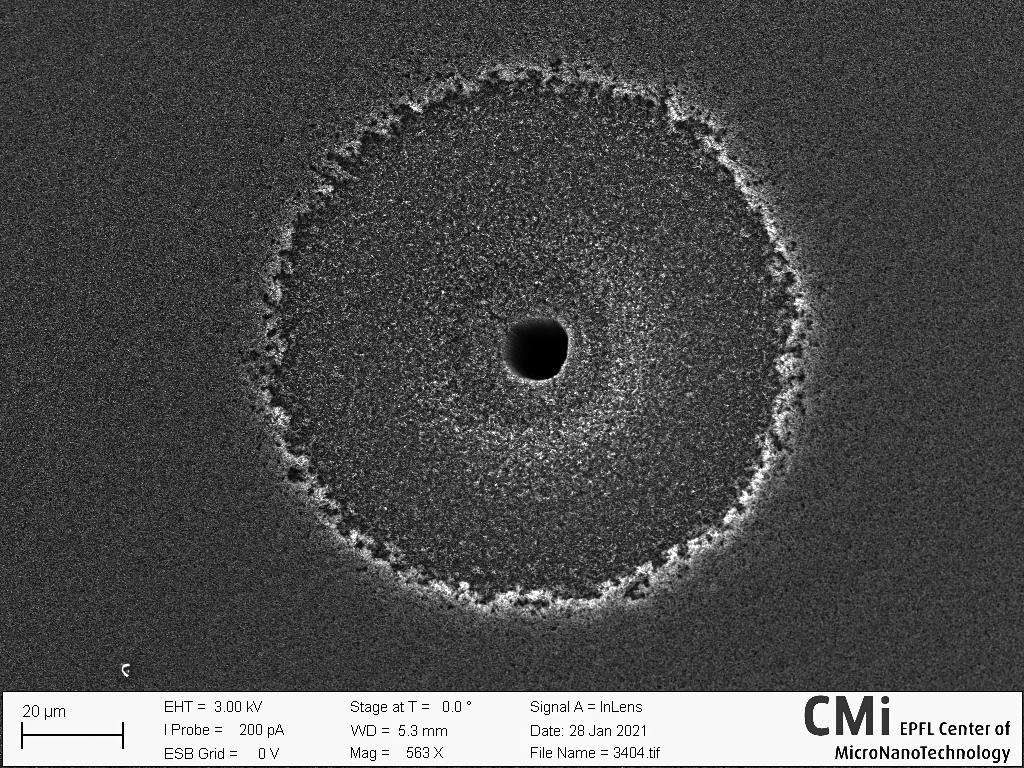
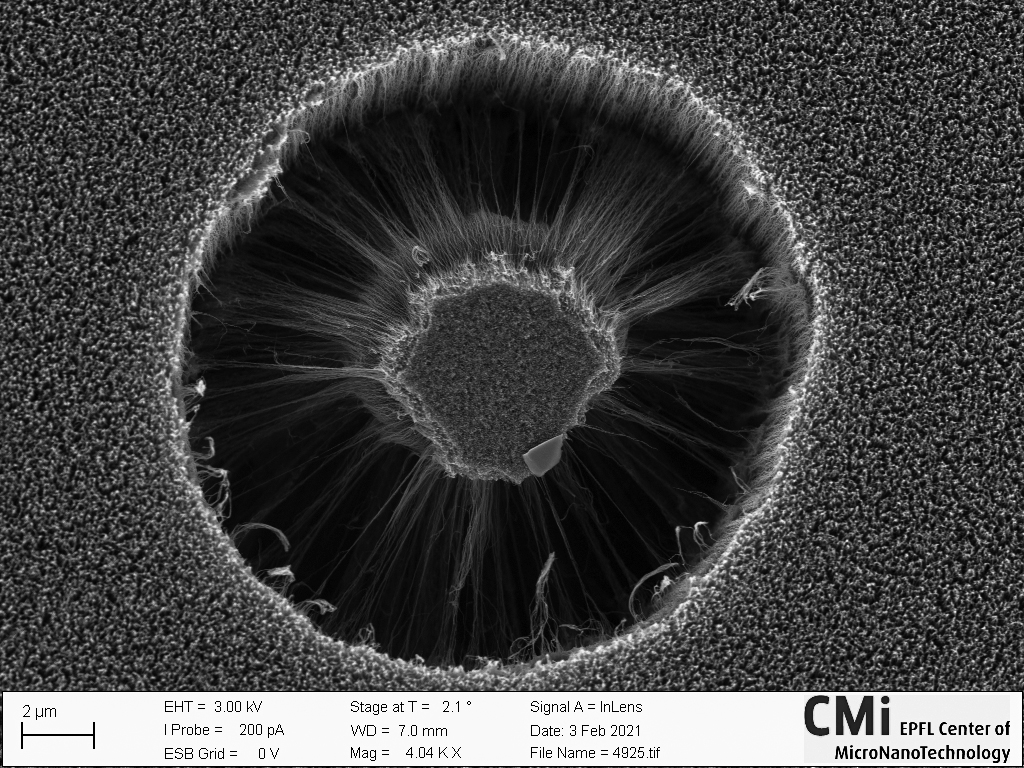
Black Hole in CMi
Pooya Dehghan, NanoLab
Nobody knows what is happening inside this black Hole. This black hole is made by work on CNT forest.
Coronapits
Alessandro Floriduz, POWERlab
In these crazy times, even pits of MOCVD-grown gallium nitride happen to be arranged in a corona shape – but don’t worry! These corona-pits won’t be harmful to any other adjacent crystal (or CMi user)! The GaN sample was grown with EPFL-LASPE MOCVD reactor and the picture was taken with CMi LEO 1550.