Back to the current year Winners
2019, December
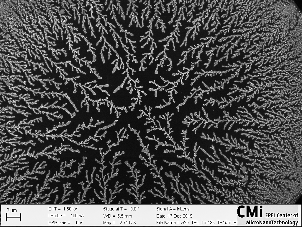
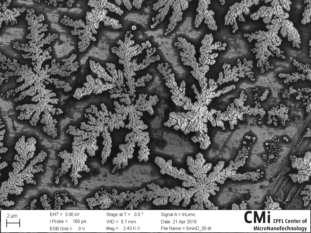
Brrr, It’s Cold in CMi
Micol Previde Massara, Q-Lab
After an HF dip, some droplets dried on my silicon wafer in the same shape that frost and ice build up on glass.
2019, November
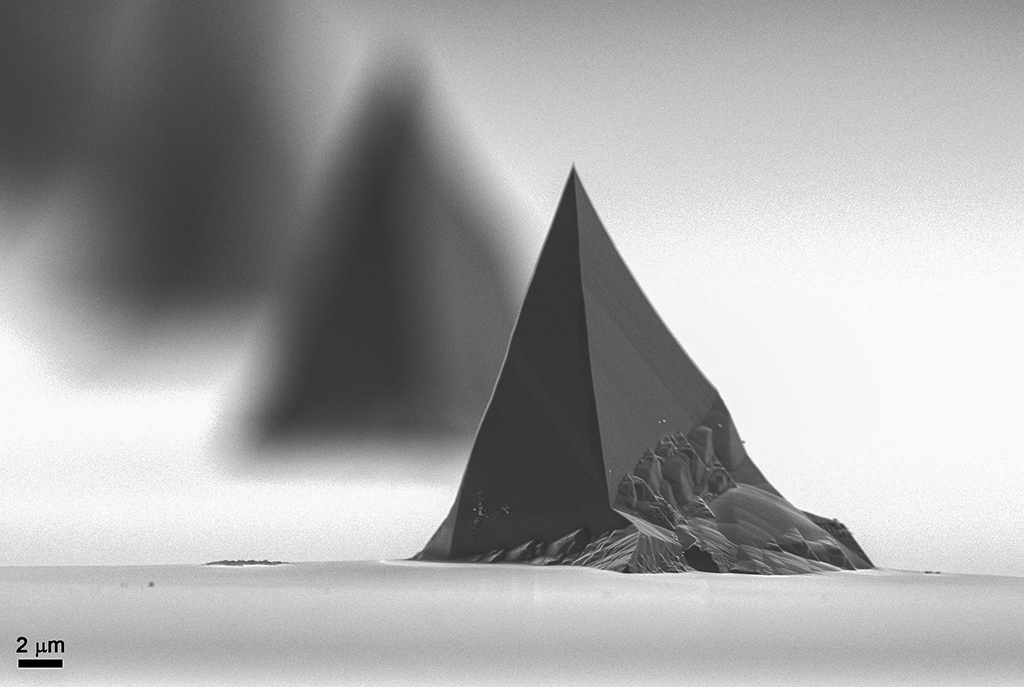
Depth of Field
Matthias Neuenschwander, LBNI
We have been walking for hours in an endless field of snow. The sun has disappeared long ago behind a thick layer of fog. We can barely see our hands. We might well be going in circles, we have lost all sense of space and time. Suddenly the mist lifts just a little. There, just in front of us, an immense structure towers in the middle of the waste land, a shard cutting through the smoothness. It’s a truly surreal sight. And behind it, though it is hard to see, there might be more. Silicon tips were created by under-etching an oxide mask in KOH. Image taken on SEM Merlin, sample held vertically and tilted 2°.
2019, October
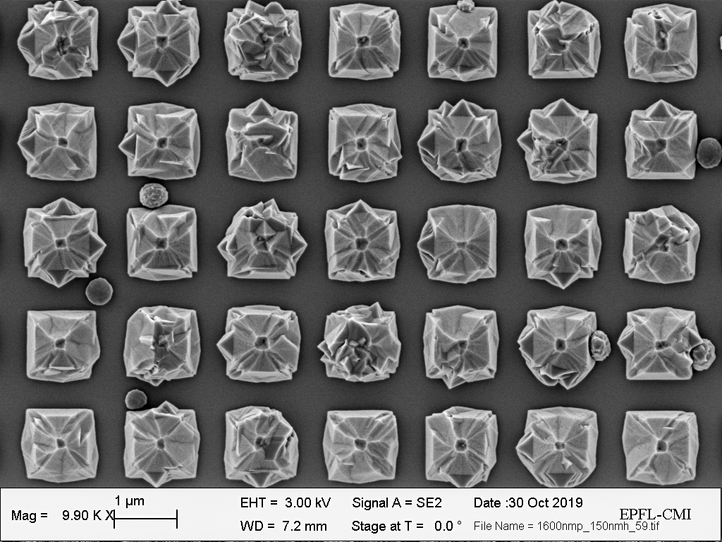
Flower Oxide Semiconductors
Virginie Lydia Pirkko De Mestral, Simon Robert Escobar Steinvall, LMSC
FOS ‘for us’ and Z. Inc. are proud to announce the release of their new generation state-of-the-art FOS1 – Flower Oxide Semiconductors.
2019, September
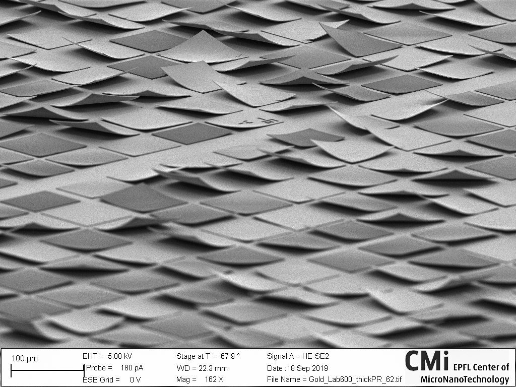
Micro Post-its
Hamed Sattari, Micol Previde Massara, Q-Lab
We address your need for post-its in the cleanroom by providing you with photoresist post-its covered by gold! After exposure with the DUV stepper and development, we deposited Chromium and Gold on our Si wafer using LAB 600H to fabricate this micro post-it array! Apparently, the stress-related issues cause many of them to peel off.
2019, August
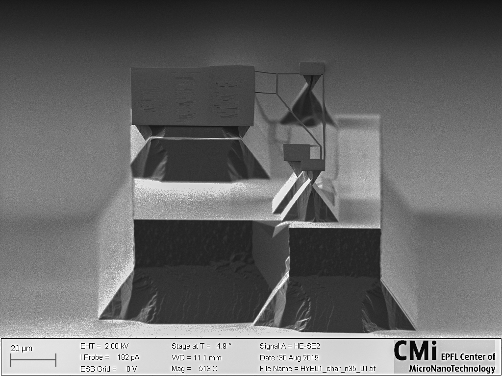
“54.74” towers
Mohammad Bereyhi, LPQM
Silicon can be etched anisotropicaly using different methods: DRIE using Bosch process and KOH. Here a silicon nitride optical cavity (patterned using ebeam lithography and dry etching) is recessed from the substrate using nested photo and electron beam lithography and deep RI etching. The recessed structure is released using KOH anisotropic etching and dried using critical point dryer. The <111> crystalline planes of Si are etched at a very slow rate compared to <100> plane. These planes are located at 54.74 degrees from the <100> planes.
2019, July
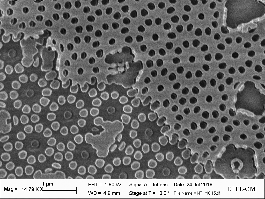
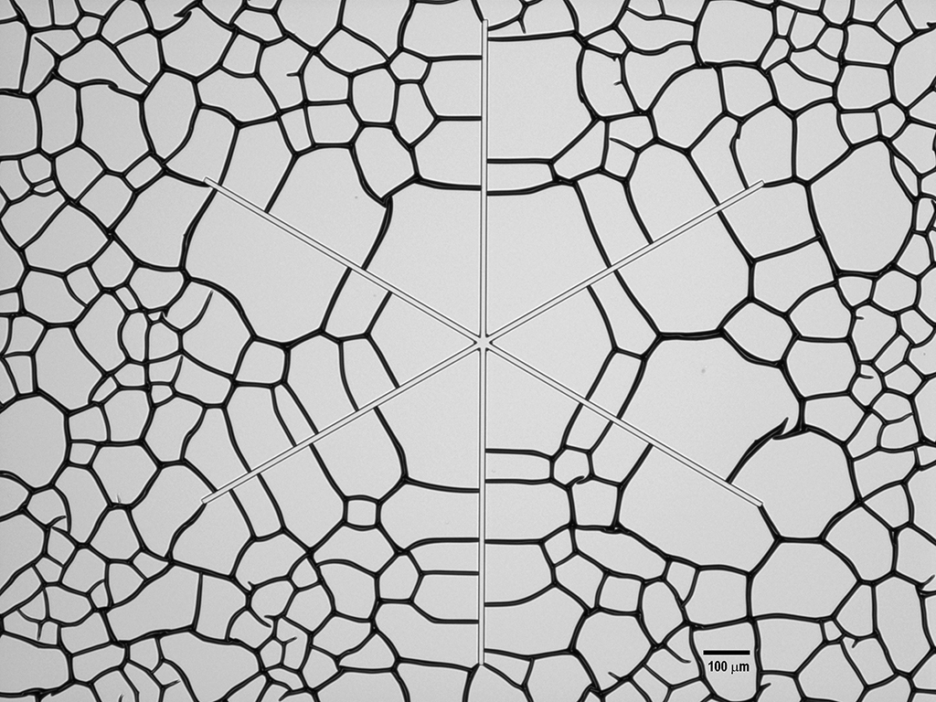
Quasicrystal fondue
Sho Watanabe, LMGN
Aperiodically arranged nanopillars get invaded by an e-beam resist fondue! This fondue now exhibits a five-fold rotational symmetry and possesses a long-range order which reflects the characteristic of the quasicrystal.
2019, June
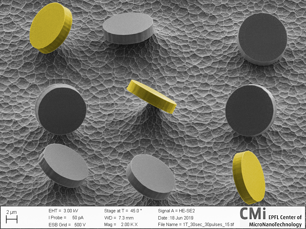
µCoins
Joffrey Pernollet, CMi
These SiO2 discs were released by an excessive isotropic XeF2 under-etching of the Silicon they were originally patterned onto. Image post-processing highlights here the winning diagonal of the most artistic landing figures.
2019, May
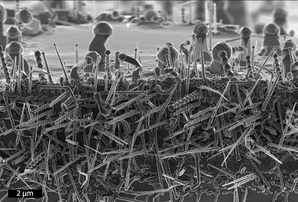
Nano Nonconformity
Simon Escobar Steinvall, LMSC
In our current experiments we are optimising the growth of zinc phosphide nanowires in arrays predefined using e-beam lithography in the cleanroom. However, the nanowires crave freedom, and as can be seen here our nanowires seem to have a will of their own. They are free independent nanowires, and ain’t no SiO2 mask gonna tell them where to grow or not! And the edge of our substrate seems to have been their location of choice.
2019, April
CNT suspension leaves
Sadegh Kamaei Bahmaei, Nanolab
CNT (carbon nanotubes) suspension on the Al foil after drop casting and drying in the air. The resulting shape looks like a leaf. It could be because of the sodium cholate, a salt used as a surfactant, when it was dried in the air.
2019, March
A metallic spider web
Lucas Güniat, LMSC
After sputtering tungsten on my PMMA-coated GaAs wafer, I found a nice web sitting at its very center. Could it be some weaving nano-insect? Turned out that we had to refute that hypothesi. Indeed, we didn’t use the SPYDER for this deposition, but the DP650… This intricate pattern revealed itself to be composed of cracks in the metallic layer (caused by a partial melting of the underlying PMMA), and by my (111) cleaving markers. Who knows, maybe the 8-leg artist is hidden somewhere on the chip, eating its prey?
2019, February
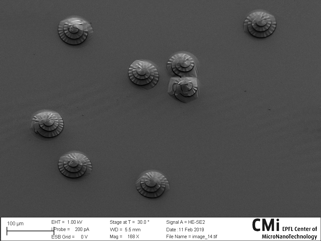
Alumina Sea Snails
Alain Yuji Takabayashi, Q-Lab
An “escargatoire” of sea snails emerges from the BEOL (Back End of Line) stack of a silicon photonics chip such that their signature spiral-shaped shells are visible under Merlin’s panoptic eye. These timid creatures only come to the chip surface when waves of HF vapor wash over pinholes in their ALD-grown alumina shells.
2019, January
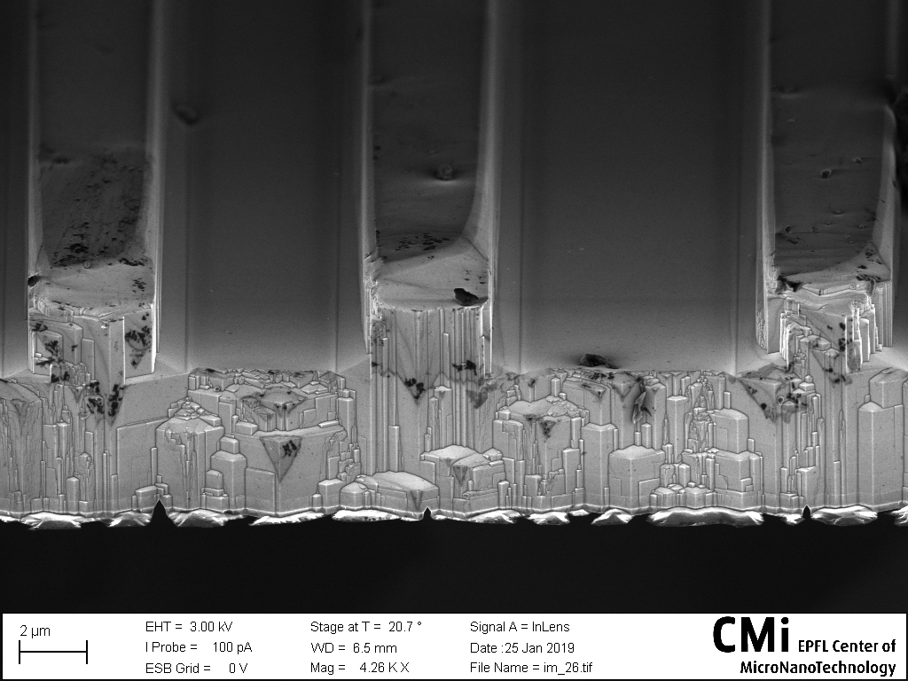
Manhattan Skyline
Riyaz Mohammed Abdul Khadar, Remco Franciscus Peter van Erp, POWERLab
This cross-sectional electron-micrograph captures the hustle and bustle of the Manhattan Skyline by night using the Zeiss-Merlin, while looking over the Hudson river. A combination of dry etch (STS) followed by TMAH wet etch on GaN epitaxial layers on Silicon exposes the crystal planes of GaN, which resemble high-rises.