Back to the current year Winners
2019, December
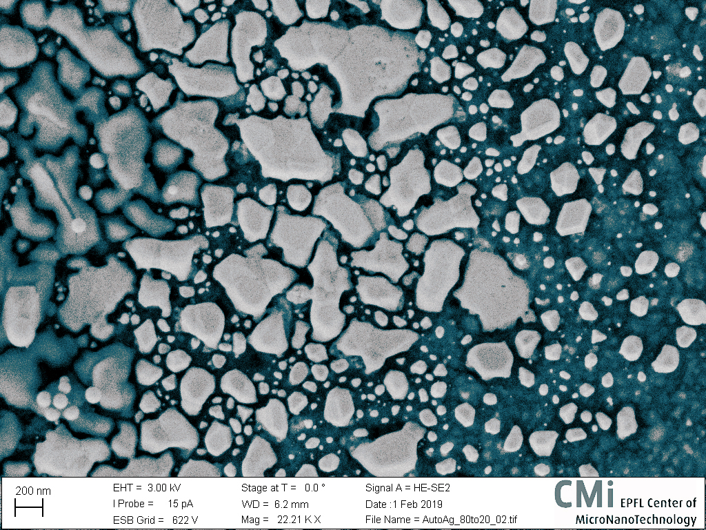
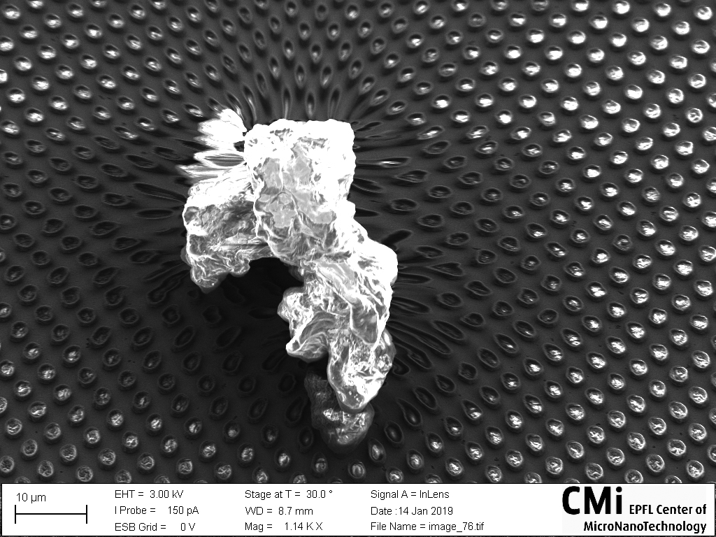
CMi Serves Caviar for the Christmas Holidays
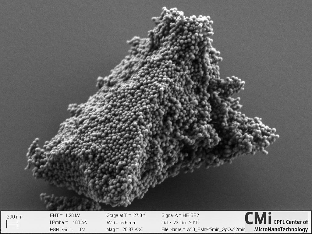
Micol Previde Massara, Q-Lab
After oxide deposition and CMP, silica nanoballs appeared on my oxide layer resembling caviar on a slice of bread.
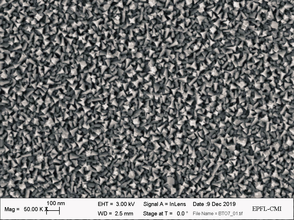
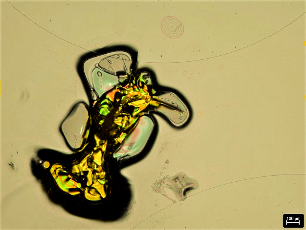
BaTi crystals
Wojciech Szmyt, EMPA
The picture shows Barium Titanate crystals grown on a silicon wafer by High-Vacuum CVD. Barium Titanate, among many other interesting applications, is useful for very high frequency electro-optic modulation, even over 40 GHz.
2019, November
Shine bright like a diamond
Gergely Huszka, Marcell Kiss, Q-Lab
Single crystal diamonds can be employed as high reflective mirrors in VECSEL-type applications due to their superior material properties, however the structuring is a challenge. We developed a standard fabrication protocol in the CMi, which enables the etching of grating structures directly into the diamond, allowing researchers to create a highly reflective diffraction grating. Such a grating was fabricated on the surface of a 6x6x0.5 mm single crystal CVD diamond and photographed as can be seen on our picture.
GaAs trees
Ayush Khurana, LMSC
Planting GaAs trees inside the nanotrenches in the CMi for Christmas! Merry Christmas in advance 🙂
Colorful Colibri
Myriam Käppeli, NEMS
Usually found in South America, this little colibri traveled all the way to Switzerland only to end up stuck in a parylene residue and then get covered by photoresist…
Who said Egyptian architects were not great visionaries ?
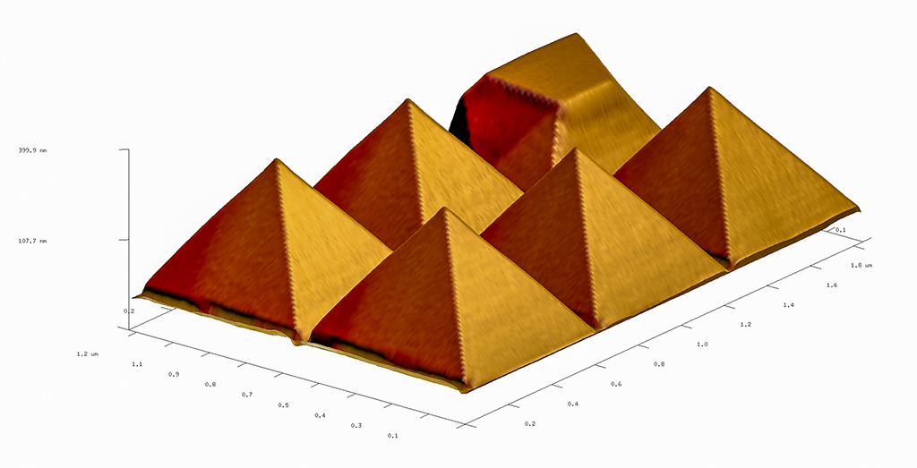
Virginie Lydia Pirkko De Mestral, Simon Robert Escobar Steinvall, LMSC
By patterning an oxide layer using ebeam lithography we can make arrays of holes for selective area epitaxy growth in our molecular beam epitaxy system. This allows growth in a regime close to thermodynamic equilibrium, resulting in the growth of nice pyramidal structures.
Magical globe
Pranav V. Kulkarni, Akshay Balgarkashi, LMSC
GaAs nanowire SEM image taken at high magnification 105kX defeating the electromagnetic disturbance in the CMi Zeiss Merlin. The shown image is the superposition of two images focused differently on the nanowire top and the bottom. This is one found with the beautiful but different growth. The globule is actually the indium droplet situated at the top. The entire arrangement is like a magical globe in which future can be seen. Indeed nano-wire research is helping to realize the quantum computing phenomena and hence the fast computing future!! I see my future in that globule, do you??
2019, October
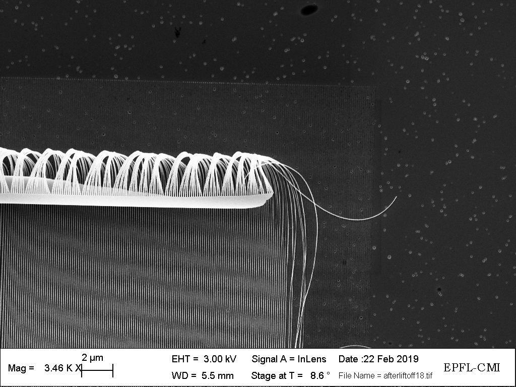
Wanted: Stuntman / Stuntwoman
Rui Ning Wang, LPQM
We are looking for somebody brave enough to do jump this 30um wide gap on a motorcycle for a CMI promotional video. The jump was fabricated by depositing and etching 800nm of stoichiometric LPCVD silicon nitride on top of a pre-patterned silicon oxide layer, the nitride layer delaminated and buckled under its intrinsic stress.
Winning at microhorseshoes – what are the odds?
Lorenz Hagelüken, LMIS1
Daniel Migliozzi, Joan Teixidor, LMIS4
Remember the good old western movies? Where cowboys would end up either in the middle of the desert or playing poker at the saloon of good old Jack, with Bobby O’Maley at the piano and Dr. Fleming selling methanol as an eternal youth elixir. And at the corner of the room, barely noticeable among this cheerful uproar, little Johnny trying to impress his secret love, Daisy, with his skills at throwing the horseshoe around the horn of the buffalo head on the wall. It looks like that period never really ended as the micro cowboys of CMi keep throwing the scalps of broken SiO2/Cr cantilevers from the MICRO-501 practicals around cantilevers that survived the terrible Valley of the KOH. According to clean room archeologists, the delaminating Cr tracks used for thermal actuation and ornamental purposes prove that this game is well spread and popular at CMi+1.

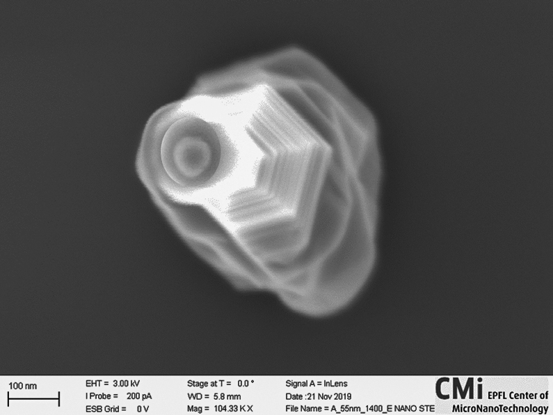
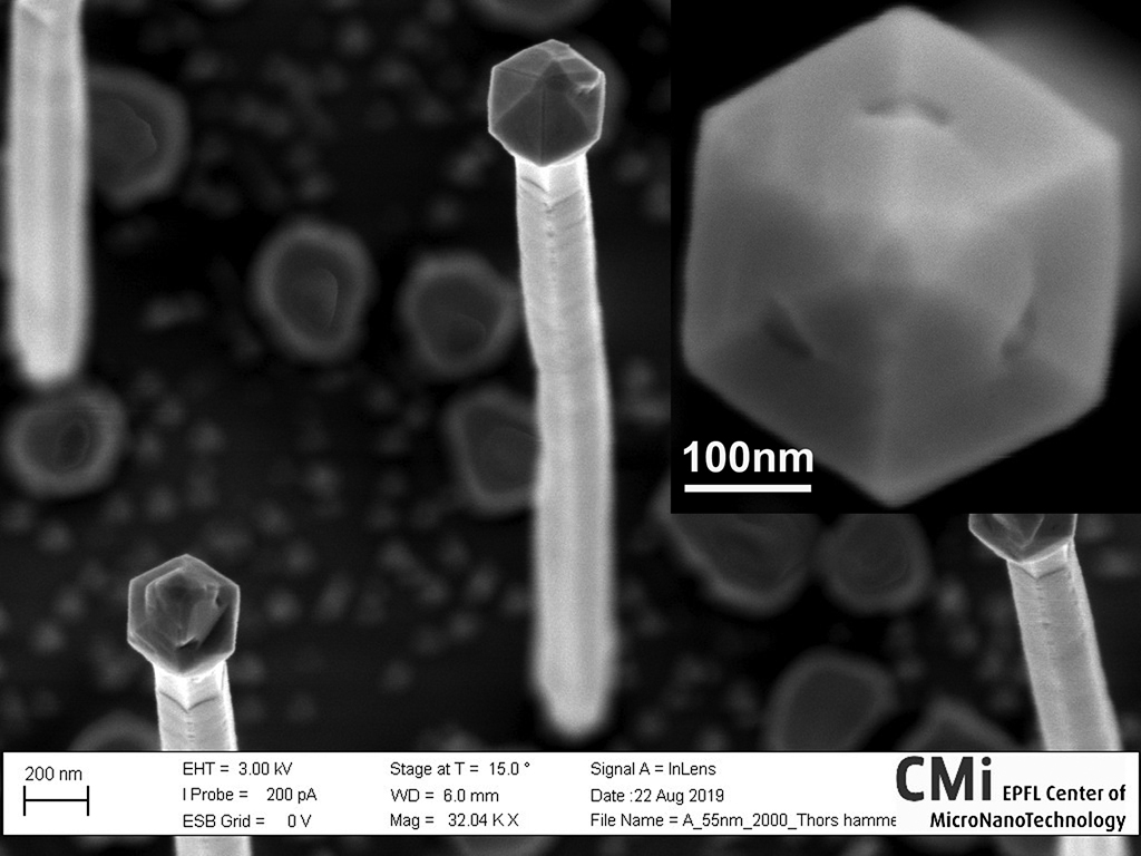
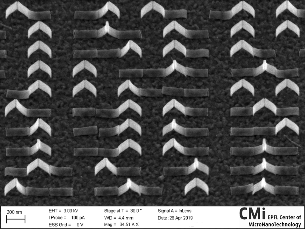
Nano Mushroom Picking
Lucas Güniat, LMSC
Boletaceae is now popping in all our forests, bringing excitement to mushroom aficionados that are eager to cook omelettes, fondue or soups with those beauties! However, it’s not the only specie we observed recently: by inserting our sample in the SEM, we were surprised to stumble upon fields of nano Armillaria Mellea! However, formed by a silicon nanopillar (AMS200 reactive ion etcher) stem and a gallium cap (deposited in a molecular beam epitaxy chamber), I’m not sure whether it’s safe to cook anything with it ! Better cross-check with my pharmacist first!
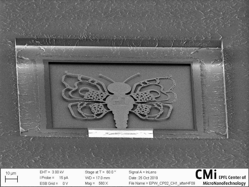
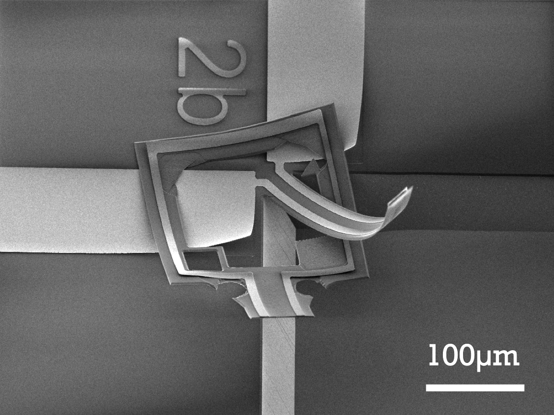
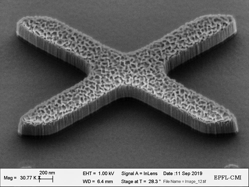
MORPHIC Butterfly
Hamed Sattari, Q-Lab
In the context of the morphic project (https://h2020morphic.eu/), we aim to introduce MEMS into IMEC’s isipp50g standard silicon photonics platform. After having the MEMS patterned in the device layer of the platform, a clean vapor HF etching process is vital to release the suspended structures safely. To prevent vapor HF from attacking the back end of line (BEOL) we initially cover the chip with an ALD Alumina layer except over the purposefully devised cavities (BEOL openings) retaining the MEMS components. MORPHIC butterfly, designed by Pierre Edinger at KTH, with large suspended wings represents a successful MEMS release process. Its right wing partially collapsed while taking this SEM image!
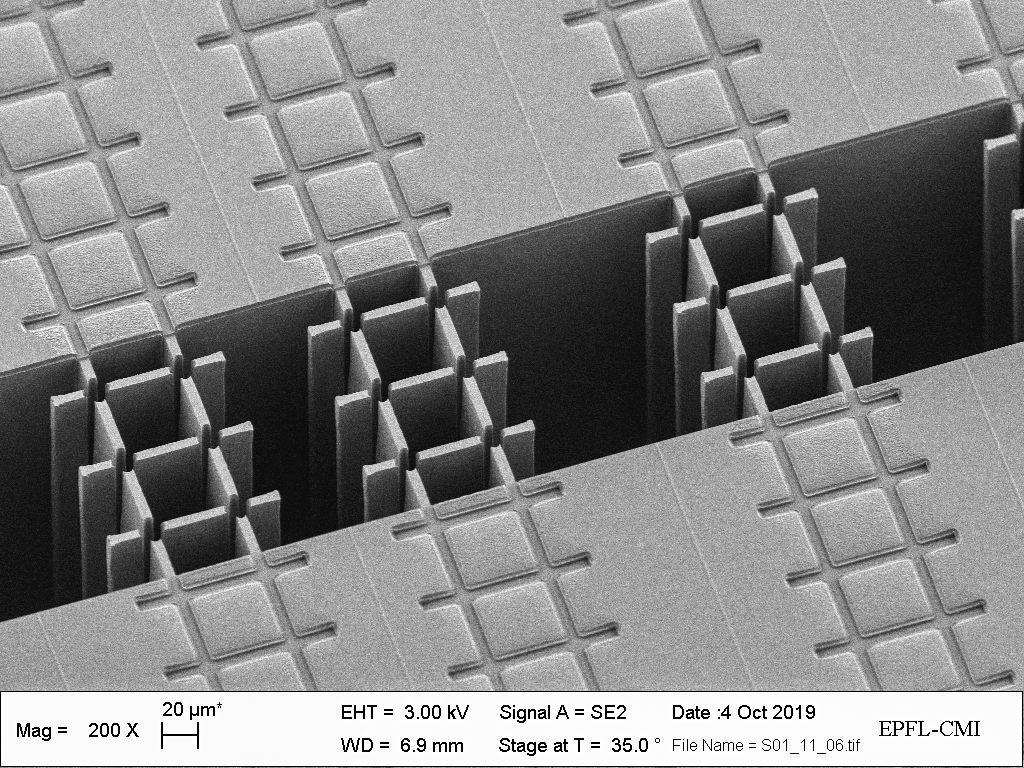
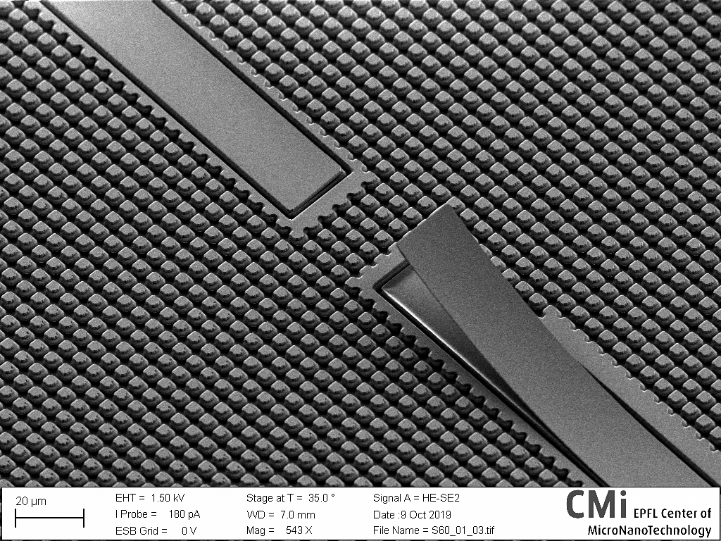
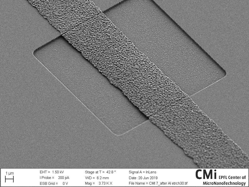
Inter-chip express railway system
Rui Ning Wang, LPQM
If you need to travel quickly from one microchip to another without getting stuck in traffic jams, the best solution is to use public transportation! These silicon railroad bridges were built by failing to remove all the silicon oxide from the trenches of the stress-relief pattern. This remaining oxide then served as an etching mask during the Bosch process.
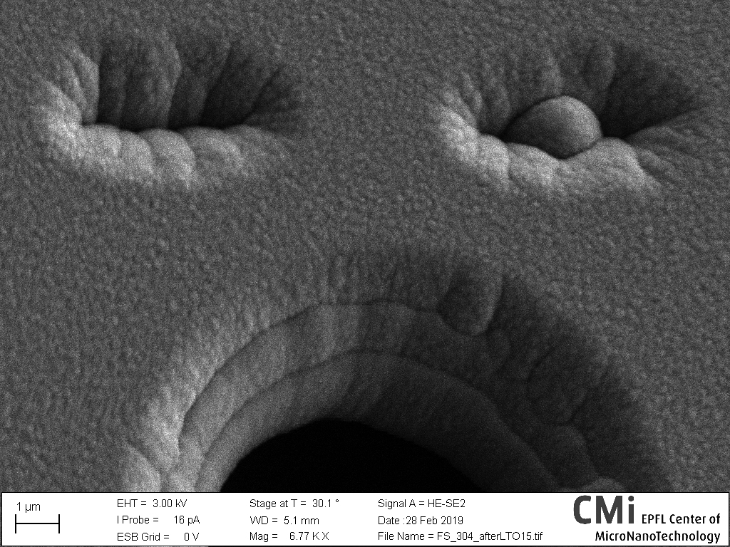
Cactus in a desert
Mohammadreza Rostami, LMIS1
Deep etching transferred the non-uniformity of the thermal resist to the thick SiO2 layer below. Since the selectivity of the resist vs SiO2 is very high, even small non-uniformities of the resist are transferred as relatively large features into the SiO2. This SEM image shows the formation of a feature that looks like a Cactus in a big desert. Primary sample consists of thermal resist on SiO2 on Si and the etching time is about 11 minutes.
2019, September
Silicon Downtown after a Vapor HF Flood
Hamed Sattari, Alain Yuji Takabayashi, Q-Lab
This low loss optical crossing “highway overpass” in our silicon photonics chip connects a modern micro metropolitan area, resilient to even the harshest of natural disasters. The suspended optical crossing is patterned in the silicon device layer and the filler tiles have been released after an HF vapor etching process due to insufficient alumina passivation.
Ferromagnetic confetti
Sho Watanabe, LMGN
Ferromagnetic confetti are released during the fabrication process of artificial quasicrystals made of ferromagnetic nanobars. These confetti pile up higher and higher as they attract each other due to their magnetic forces.
For the planet
Reza Soleimanzadeh, POWERLab
Mehdi Naamoun , Lake Diamond
The eyebrow-raising news about global climate change coming from the recent scientific studies predict that melting of Antarctica could contribute somewhere between about three to 16 inches to the world’s sea levels rise by 2100. This picture is a not just a SEM image of a diamond chip grown at Lake Diamond SA, but it is also a reminder of the icebergs, how fast they are melting and how worrying the consequences are. Let’s do something for the planet.
A tetrapod nano-starfish
Hernan Fernando Furci, Q-Lab
The ground-breaking point of this photo is not only that this is the tiniest ever observed starfish, but also that this invertebrate was observed lying directly on silicon (in contrast to all other known species of this family that have only been found lying on silica granulate, commonly known as “sand”). Most of the body of this specimen is made of M108Y exposed with DUV Stepper, except for a thin layer in contact with the ground made of BARC opened in SPTS with He/H2/C4F8 chemistry.
Modern Art on Silicon
Mohammad Samizadeh, POWERLab
I’m pleased to present the latest artistic masterpiece of the anonymous artist BankSi. The audience say it is showing the moment of Big Bang, however, BankSi said he had absolutely no idea while he was paining this: “it’s just a modern art,” he said. The base price for this amazing paint is 100 kCHF. On top of this price, however, you would need to buy a nice microscope, since it has been painted in micro-scale! This is basically an AZ photoresist on a Si substrate. On top of this photoresist, there was a metal layer which was completely etched by IBE, making the photoresist underneath so nice. The picture has be taken by optical microscope in Z11.
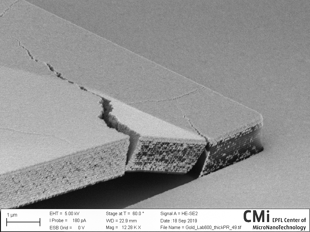
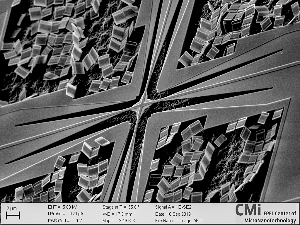
Micro-Iceberg in a Golden Ocean
Micol Previde Massara, Hamed Sattari, Q-Lab
Global warming should be taken seriously even in the cleanroom! In order to test the lift-off process with DUV photoresist, we deposited Chromium and Gold on our wafer in LAB 600H. Due to a poor photoresist adhesion and the stress induced by the deposited film, our photoresist iceberg cracked, and it is going to split into pieces in the golden ocean.
2019, August
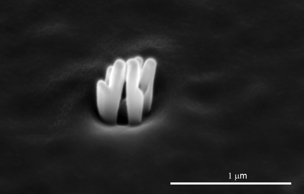
Crystalline Agaricus Bisporus
Akshay Balgarkashi, Santhanu Ramanandan, LMSC
While attempting to grow nanowire heterostructure arrays on a rainy day, our molecular beam epitaxy system could not resist producing nano-mushrooms. Unlike the ones growing in a garden, these mushrooms show pristine crystalline caps which could be observed by tweaking the collector bias and capturing the images using signal mixing from InLens and SE2 detectors. Though they might be tempting, it’s a pity they are not edible.
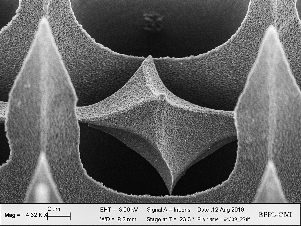
Geometry in balance
Riccardo Callegari, CERN
The XeF2 over etching always creates original geometric shapes in silicon. It is not uncommon to find precariously balanced sculptures as the one shown in the picture, taken with the LEO.
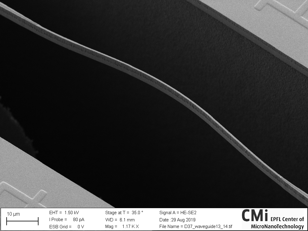
Don’t look down!
Rui Ning Wang, LPQM
This suspended SiO2 waveguide is about 1um wide and 4um thick, and spans a gap 300um long. If you are a photon, mind the edge when crossing because we didn’t put any safety handrails. And it’s a dizzying fall of 250um high into a sea of black sticky SEM adhesive.

ALD showers bring August flowers
Michele Bozzetti, INE
The sample is a porous matrix of Carbon Black and PTFE where ZnO Atomic Layer Deposition was performed using the “Beneq TFS200” tool from CMI.
2019, July
Ephemeral Micro Skyscrapers
Joffrey Pernollet, CMi
These rectangular protruding structures are believed to be NaCl crystals, that built-up on Soda Lime glass surface (15% of Na2O) after Cl2/O2 reactive ion etching of a chromium layer, with a significant over-etch period. The chromium layer is visible in the background, with the photoresist mask still on top. These crystals grew up fast, much taller than all layers on the substrate, and forming a tiny isolated city of micro skyscrapers originated from nowhere. They remained ephemeral, as they all completely vanished after DI water rinse of the sample.
2019, June
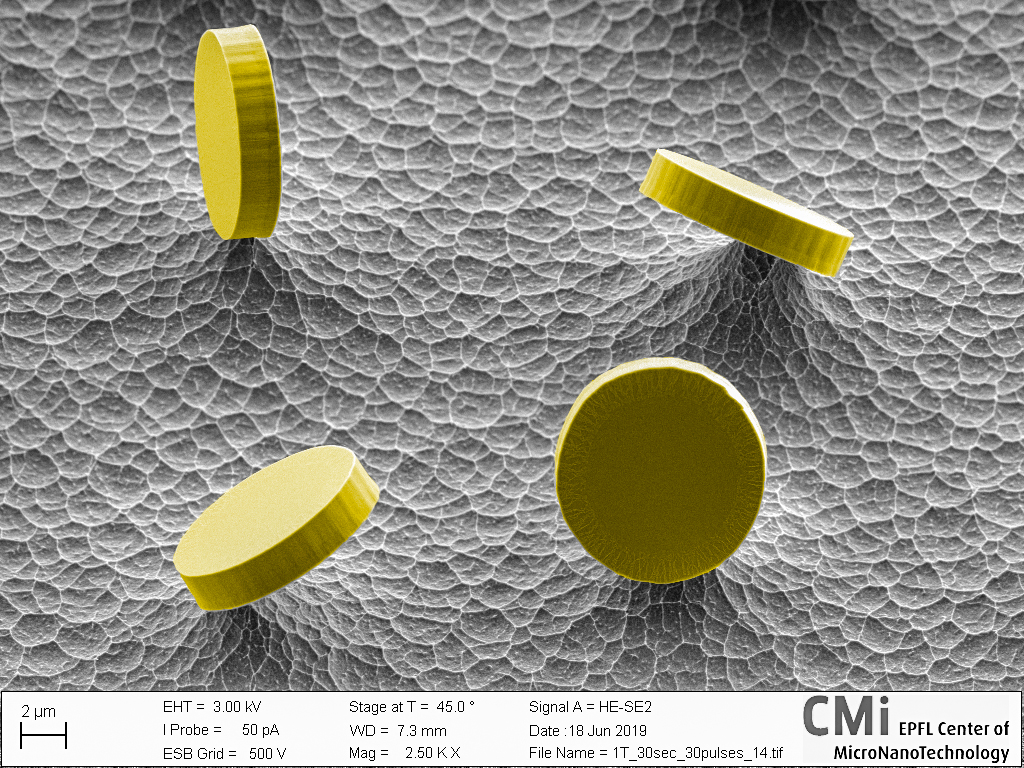
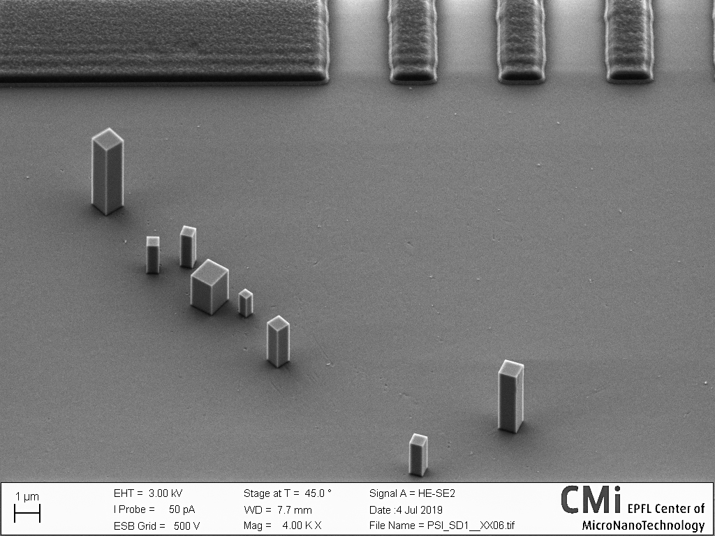
µCoins 2
Joffrey Pernollet, CMi
These SiO2 discs, with surprising standing positions, were released by an excessive isotropic XeF2 under-etching of the Silicon they were originally patterned onto.
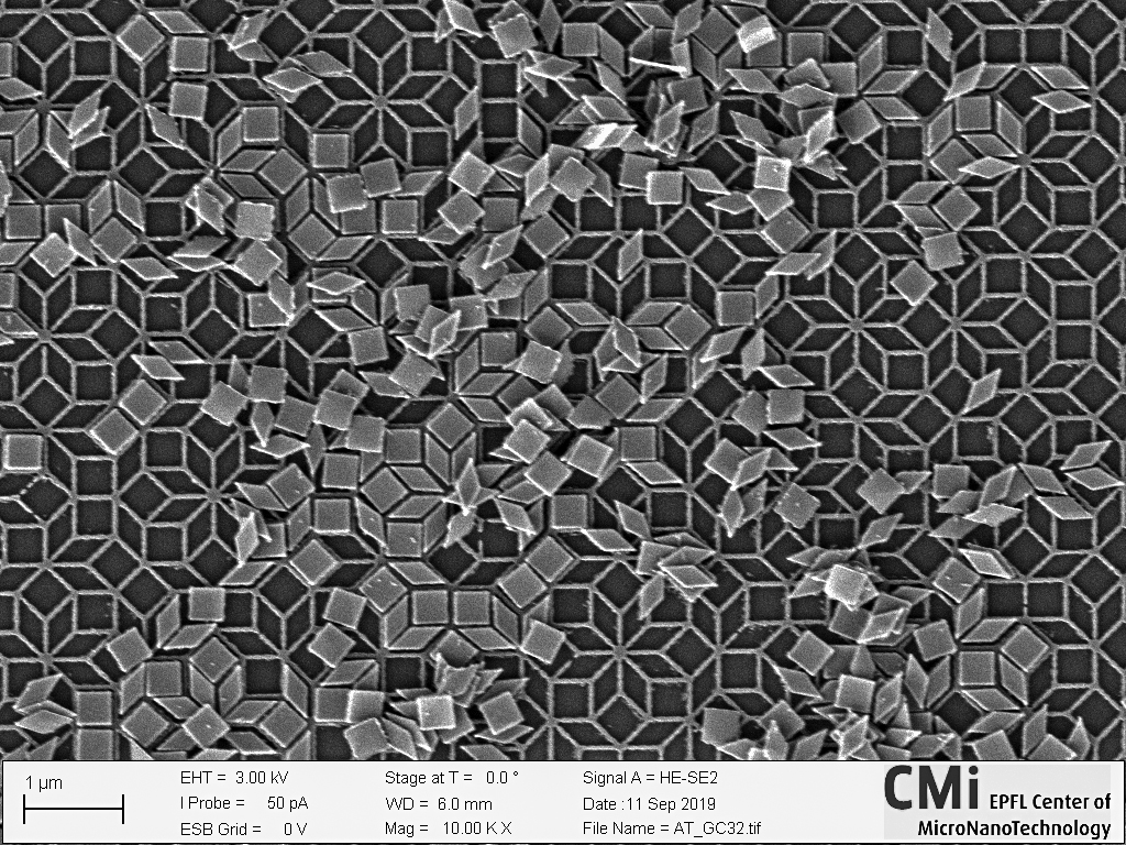
µ-Stonehenge
Andrea Giunto, LMSC
Surface contamination caused this weird formation during GeSn sputtering on a Ge substrate. Microcrystals assembled to form what resembles a µ-Stonehenge, seen from the top. Why the adatoms organized in this configuration remains unknown. Will the resolution of this mystery provide source of inspiration for understanding the origin and use of the real, meter-sized Stonehenge?
Stand Tall
Mohammadjafar Bereyhi, LPQM
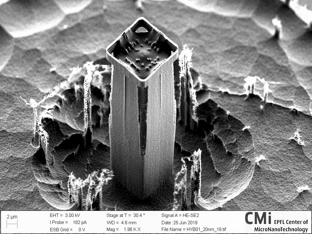
It’s quite difficult to stay strong when everything is being attacked by high energy plasma in a dry etcher, unless you have a strong wall to lean on! This picture is from an alignment mark that is used to align two ebeam patterns using negative resist (FOx 16). As a result the ebeam search area is exposed to electrons and the resist is partially exposed and hardened after development in that region. The ebeam mask is used to do silicon etching using BOSCH process and the marker has been protected with the partially exposed resist during the DRIE process. The ebeam search pattern for alignment is visible on top of this “tower” (series of equally spaced concentric dots).
Micro Suspension Bridge
Amir Youssefi, LPQM
A tiny (80nm thick) Aluminium bridge suspended on top of a shallow (150nm depth) trench in the Si substrate. This structure is used to form a mechanically compliant superconducting parallel plate capacitor as a building block of the quantum electromechanical systems.
2019, May
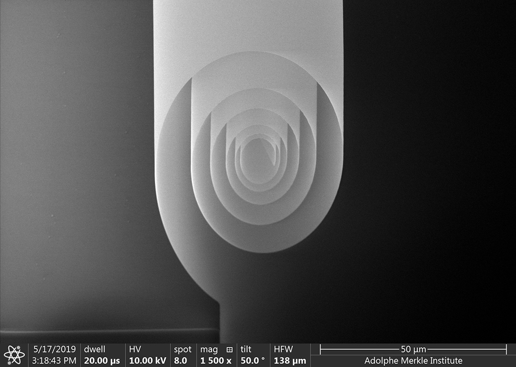
µ-Spiral
Esteban Bermudez, AMI Friburg
This glass micro-spiral resulted from a stress-driven mechanism when releasing a 60 nm SiO2 thin film from the substrate. Sample patterning, thin film depositions and etching steps were carried out at the CMi, while the SEM imaging was performed at the Adolphe Merkle Institute in Fribourg.
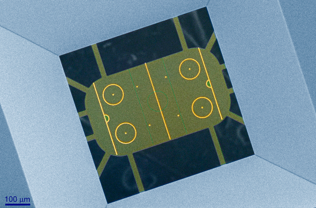
It’s hockey time!
Matthias Neuenschwander, LBNI
For the micro-world cup, an ice-rink fount its way onto my wafer. It is suspended in a silicon frame and consists of nitride-polymer-nitride sandwich structure. The line-markings are made of poly-silicon (blue-ish) or gold (yellow). Even though they are situated below the first nitride film, these lines can be seen with the SEM using a relatively high voltage. The colour is obtained by overlaying an optical microscopy image in Photoshop.
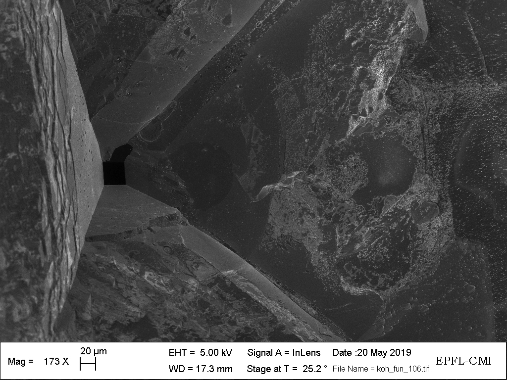
Ancient corridor
Andrey Chernev, LBEN
Si wafer was processed at CMi (photolithography), then KOH etched and imaged with SEM. SiN mask detached while wet etching, so the step was not successful, however this caused some beautiful designs.
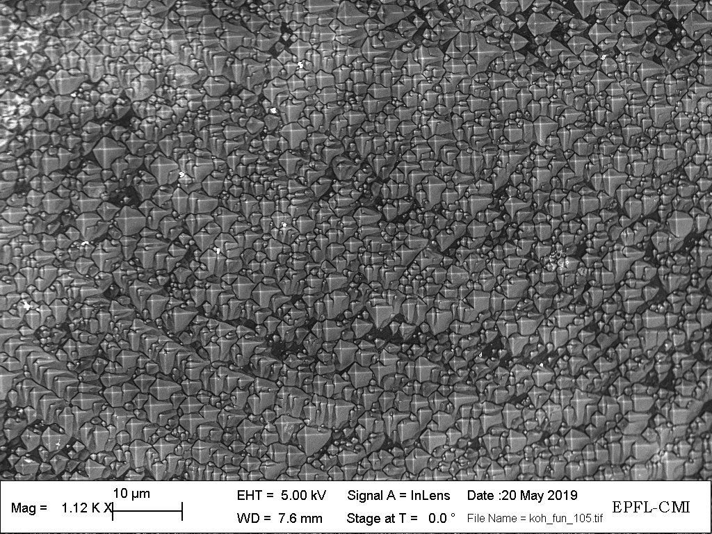
Grandveaux terraces
Andrey Chernev, LBEN
Si wafer was processed at CMi (photolithography), then KOH etched and imaged with SEM. SiN mask detached while wet etching, so the step was not successful, however this caused some beautiful designs.

Micro black hole
Henry S.C. Yu, LMIS1
This is a Quick-Stick structure formed after O2 plasma treatment in the Tepla tool at BM+1. It seems some of the Quick-Stick around a chip on a Si wafer melted and splashed around to form small droplets during the process.
2019, April
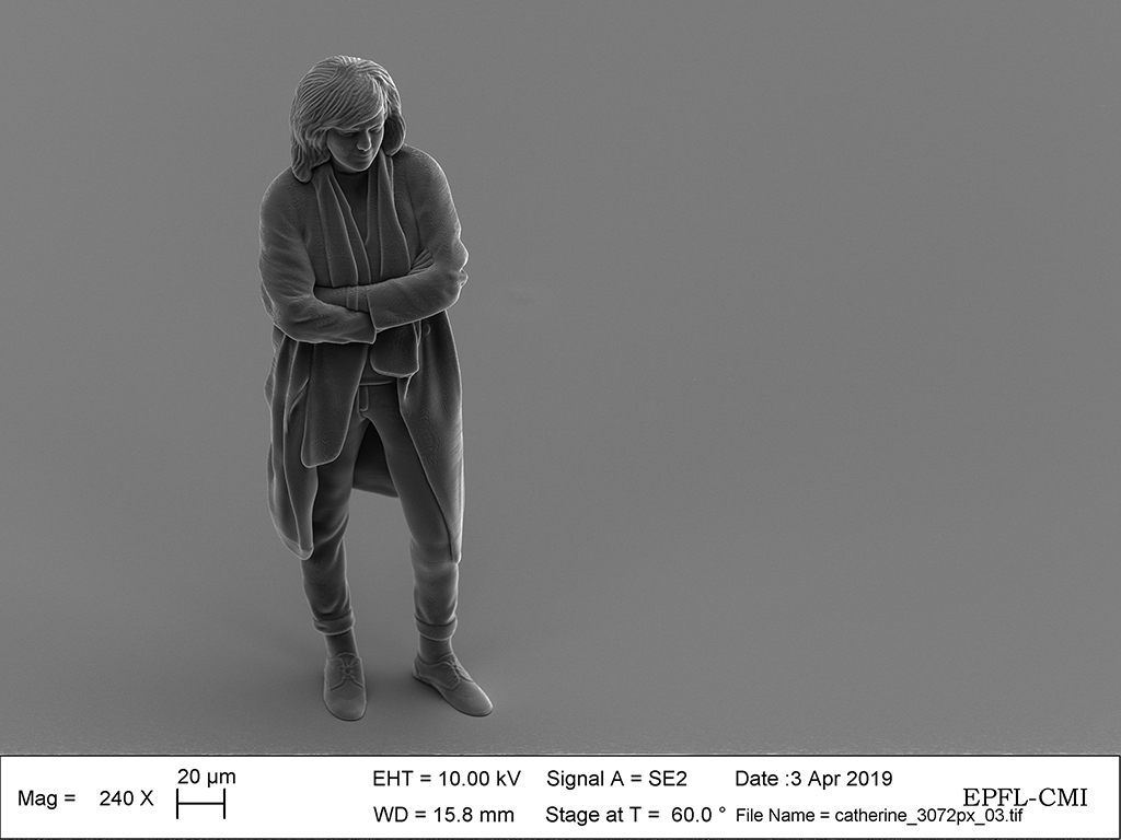
Catherine
Catherine Leutenegger, C.L.
Zdenek Benes, Julien Dorsaz, CMI
Microscale miniature of Catherine Leutenegger’s full body and one of the worlds smallest statues of a human form, the 300um-tall figurine is printed using laser-based two-photon polymerization of a UV-sensitive epoxy resin on a Nanoscribe tool at CMi. 3D scan by Minimoi, Renens.
Renaissance style sapphire mullion window
Clémentine Lipp, LMIS4
Al2O3 alignment marks turn into beautiful renaissance style windows when the process contains an underetching step. Who would have guessed that Windows 11 would be Windows Sapphire?
The Rise of the Undead HSQ
Aleksa Djorovic, NAM
After a seemingly standard E-beam exposure, something extraordinary occurred to the HSQ mask. The HSQ rebelled! Not only did the smaller rectangular strips migrate towards their longer counterparts – but then they started to rise! Building nano-bridges of HSQ not more than 40 nm high – pulling each other up to create a spectacular sight of 3D structure from extremely thin layers of HSQ – reminiscent of the HSQ trying to rise from the wafer… HSQ mask on chromium and aluminum.
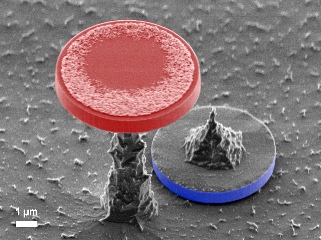
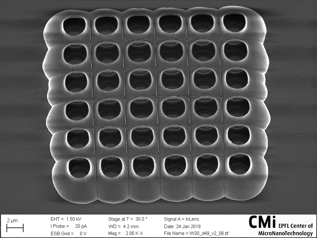
How it’s made: Micro Push Pins
Teodoro Graziosi, Q-LAB
Here are two single crystal diamond “micro push pins”: the red one is not yet ready and it will need more etching before being used. These “push pins”, or more precisely micro-disks, are fabricated starting from a single crystal diamond plate. After electron-beam lithography and vertical etching in a high bias oxygen plasma, the release is performed with a high power, high temperature, and zero bias oxygen plasma. The blue micro-disk was etched too long and it is unfortunately only good to hang microscopic posters.
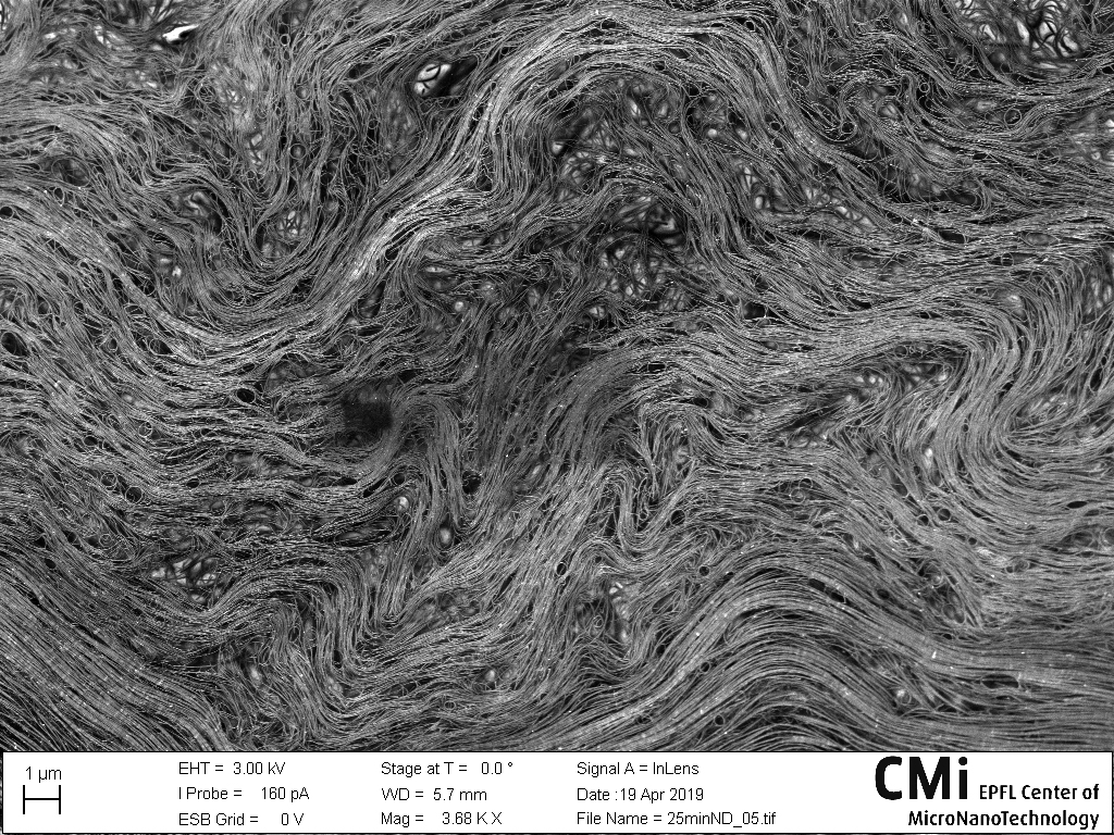
CNT roots
Sadegh Kamaei Bahmaei, Nanolab
CNT (carbon nanotubes) suspension on the AL foil after drop casting and drying in the air. Nanometric CNTs are similar to the roots of trees, in this case, “CNT roots”.
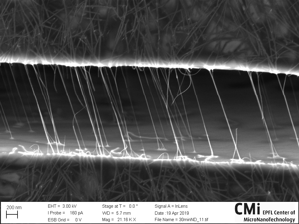
CNT bridges
Sadegh Kamaei Bahmaei, Nanolab
CNT (carbon nanotubes) suspension on the AL foil after drop casting and drying in the air. Nanometric CNTs bridge 2 different networks of agglomerated CNTs. It looks like a roof which is supported by the CNTs posts.

The Scream
Clémentine Lipp, LMIS4
Edvard Munch understood. When the energy deposited by an SEM into a non-conductive wafer exceeds the wafers capacity to absorb it, the wafer screams!
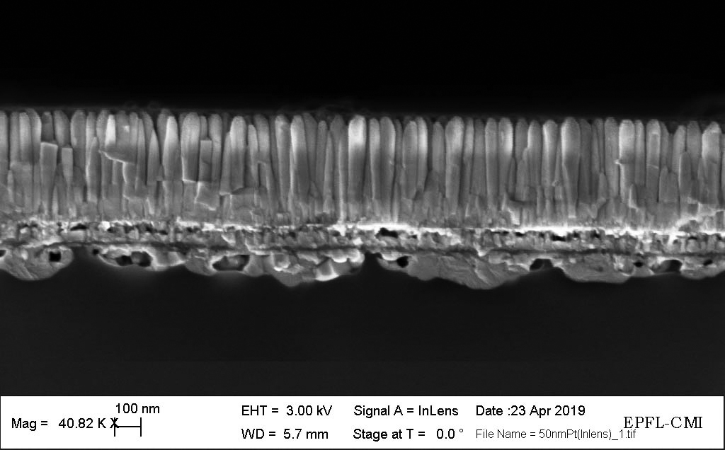
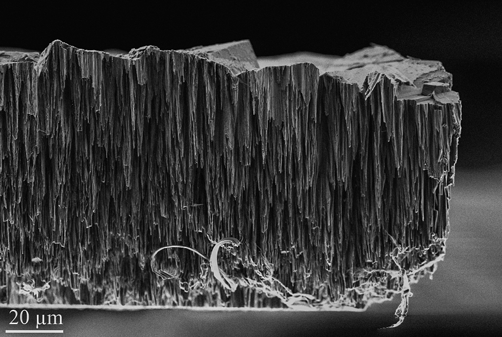
Metallic toothbrush
Romain Charfaz, NEMS
This picture is a cross-section observation of a 450 nm PBZT (PbBaZrTiO) columnar structure grown by PLD (Pulsed Laser Deposition) on a 50 nm Platinum layer (on an Si substrate).
2019, March
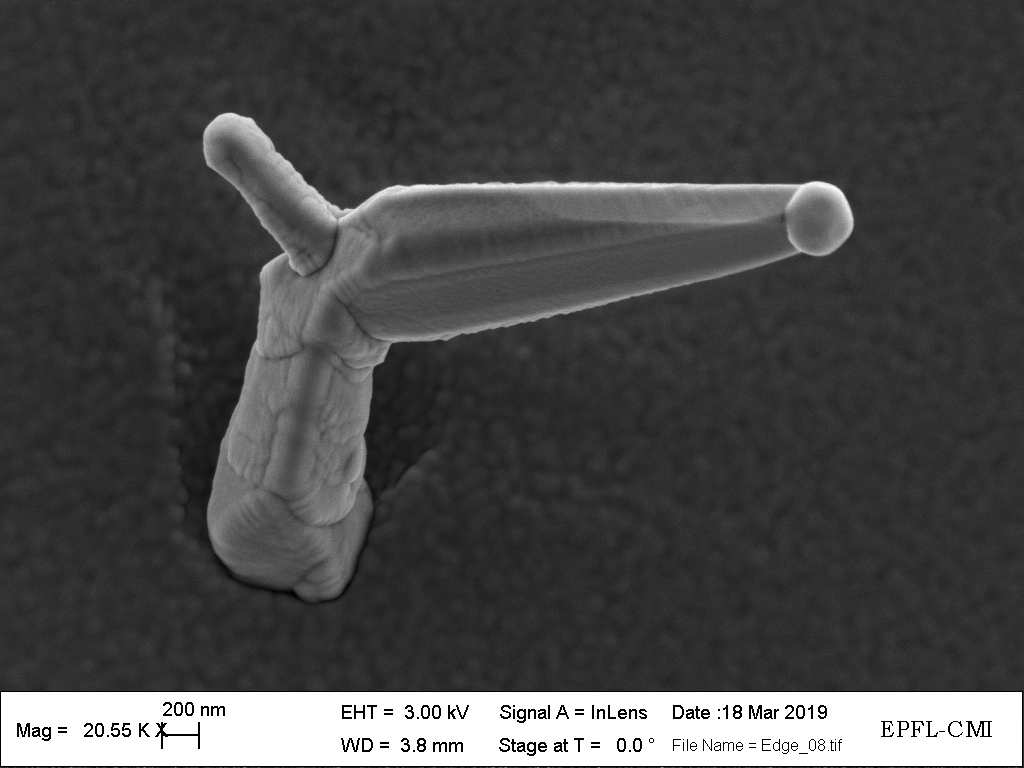
What do you see?
Simon Robert Escobar Steinvall, LMSC
When investigating bottom up growth of nanostructures, the growth results can have an effect similar to a Rorschach test. What does this SEM image of a vapour-liquid-solid grown zinc phosphide nanostructure resemble to you? Is it a nano-gun of the future? Rudolph the indium nosed reindeer? A long nosed dog with pointy ears? A unicorn? The possibilities are endless!
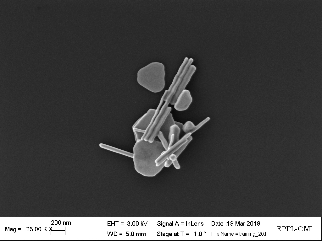
Seated man with banjo
Ana Conde Rubio, LMIS1
Scanning Electron Microscope picture where you can see an aggregation of Au particles of different shapes that look like a seated man playing banjo.
Aluminum neurons
Kamila Guérin, LPMV
This optical microscope image shows the edge of the wafer covered with Cr/Al/Au. During the development of AZ9260 on the other side of the wafer, aluminum layer got “attacked” by the developer revealing neurons-like artifact.
A tungsten new logo?
Lucas Güniat, LMSC
Wanting to deposit tungsten using the room temperature_fast recipe on the DP650 sputtering machine instead of the room temperature_uniform lead to a cracking of my 100nm-thick PMMA layer! Luckily, the EPFL “logo” that I exposed is intact, surrounded by this intricate cracky-pattern. It seems that this new identity has been built to stand the test of time!
2019, February
Distant planets
Anastasiia Glushkova, LPMC
The SEM image of the curved glass with grown crystals of methylammonium lead bromide resembles a surface of an unknown planet interesting for research.
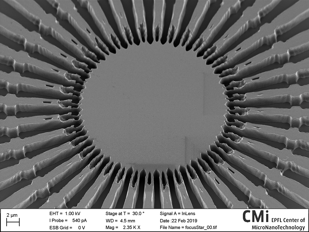
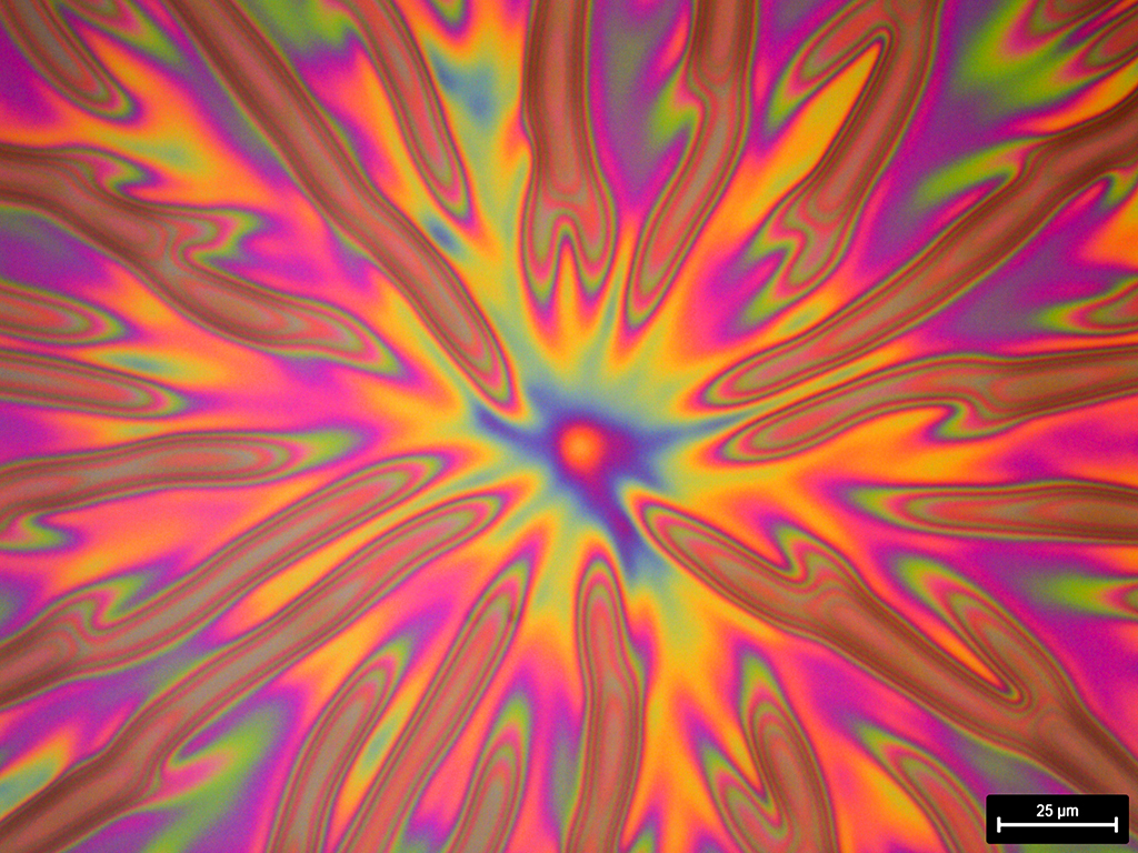
Focus star
Georges-André Racine, Niccolò Piacentini, CMi
Proximity-induced interference modifying the center of a “focus star” test structure. AZ MIR701 resist on EVG150/MA6genIII, SEM Zeiss Merlin.
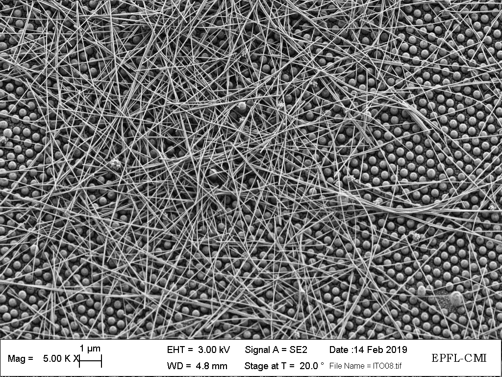
Silver amor
Nuño Amador Mendez, Wonjong Kim, LMSC
In the picture we can see two different kinds of nanowires. In the background are the InP nanowires encapsulated in SU8 with an ITO layer on top, for solar cell applications. The dispersed nanowires in the front are made of Silver, and the purpose of them is to make a transparent contact on the top. This beautiful union between nanowires was observed on Saint Valentine’s day.
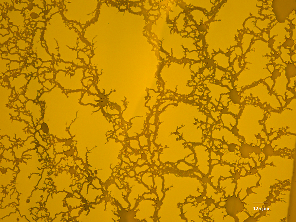
Melting of glaciers
Debdatta Ray, NAM
Global warming has not only taken a toll on the world climate but has also made its presence felt on my wafer with the silicon substrate. The glaciers are made of gold and silver alloy, deposited and alloyed in CMi cleanroom, whereas the sea water is a combination of silicon, gold and silver.
CMi Microlace, AOP
Joachim Ciers, LASPE
The centuries old artisanal technique of lace is brought to the microscale at CMi. These 50 nm wide wires are lifted-off from an optical grating coupler on a GaN waveguide. The structures are fabricated with e-beam lithography and metal evaporation.
Quand tout est à recommencer
Clémentine Lipp, LMIS4
This image represent your expression under your face mask when you realize the whole process is to be started all over again. Luckily it wasn’t the case of this vertical cell trap fabricated in a glass substrate using a patterned alumina layer, HF etching and a deposition of low temperaturevv oxide.
2019, January
Miniaturized Rolex learning center
Nicolas Maïno, LMIS4
As for the original, successive layer of silicon dioxide, titanium and gold concretes were applied through sputtering side wall re-deposition on a photoresist scaffold. The result is an open free-standing roof bringing light to the inner patio of platinum.
The Matrix
Dorian Herle, Q-LAB
It was a perfectly normal day when I sat down as usual in front of the CMi SEM tool. Then it happened. An odd-looking object began to deform space. Didn’t I take the blue pill this morning?! Mr. Smith smiled: “What you are seeing is called charging”. I nodded politely: “Of course.” Everything in this world could always be explained in rational terms. I was a fool. Yet, for the first time in my existence I could not help but question, if what I was seeing, or believing to see, was actually real.
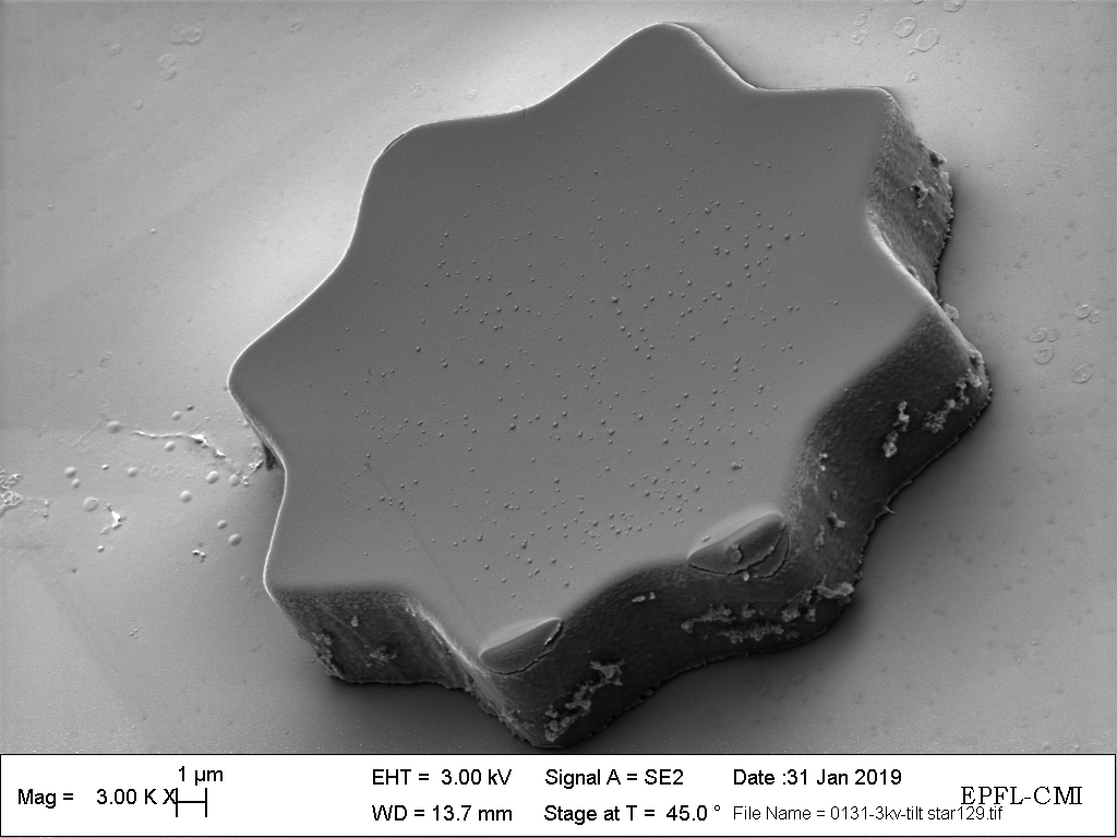
A micro-star is born!
Zhiwei Yang, Xia Liu, LMIS1
This is an SEM image that shows a pre-patterned SU-8 star transferred onto another glass substrate using laser-induced forward transfer (LIFT) technique.
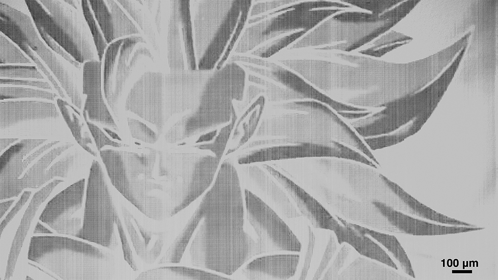
Goku SSU8
Riccardo Dainese, LSBG
There is always lots of unused space between microfluidic molds on a wafer. So I decided to put this space to a good use and pay my tribute to a legend. The image is composed of SU8 micro-pillars whose cross-section is directly proportional to the gray-scale pixel value in the corresponding digital image. The image was taken with one of the microscopes of the CMi. The R2-D2 made with the Nanoscribe is cool, but Goku SSU8 is super.
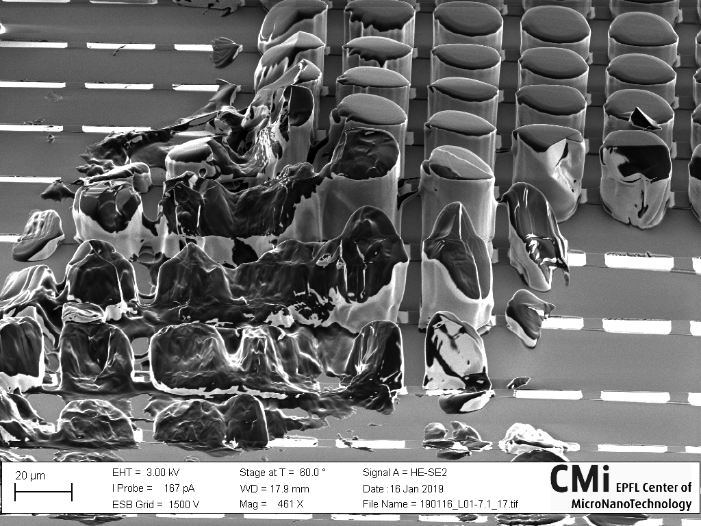
Melted SU-8 pralines
Kevin Keim, CLSE
These Suisse platinum-coated SU-8 pralines, were left to close to the heating after Christmas. Over the break, the SU-8 melted away and left this impressive image.