Back to the current year Winners
2016, December
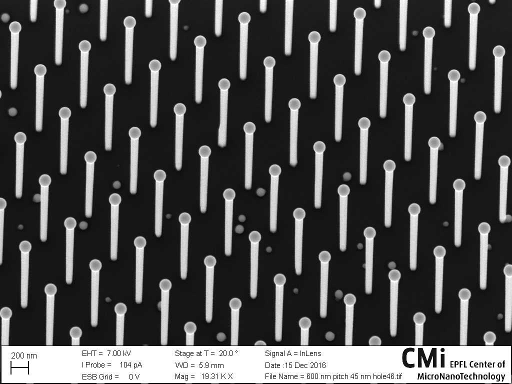
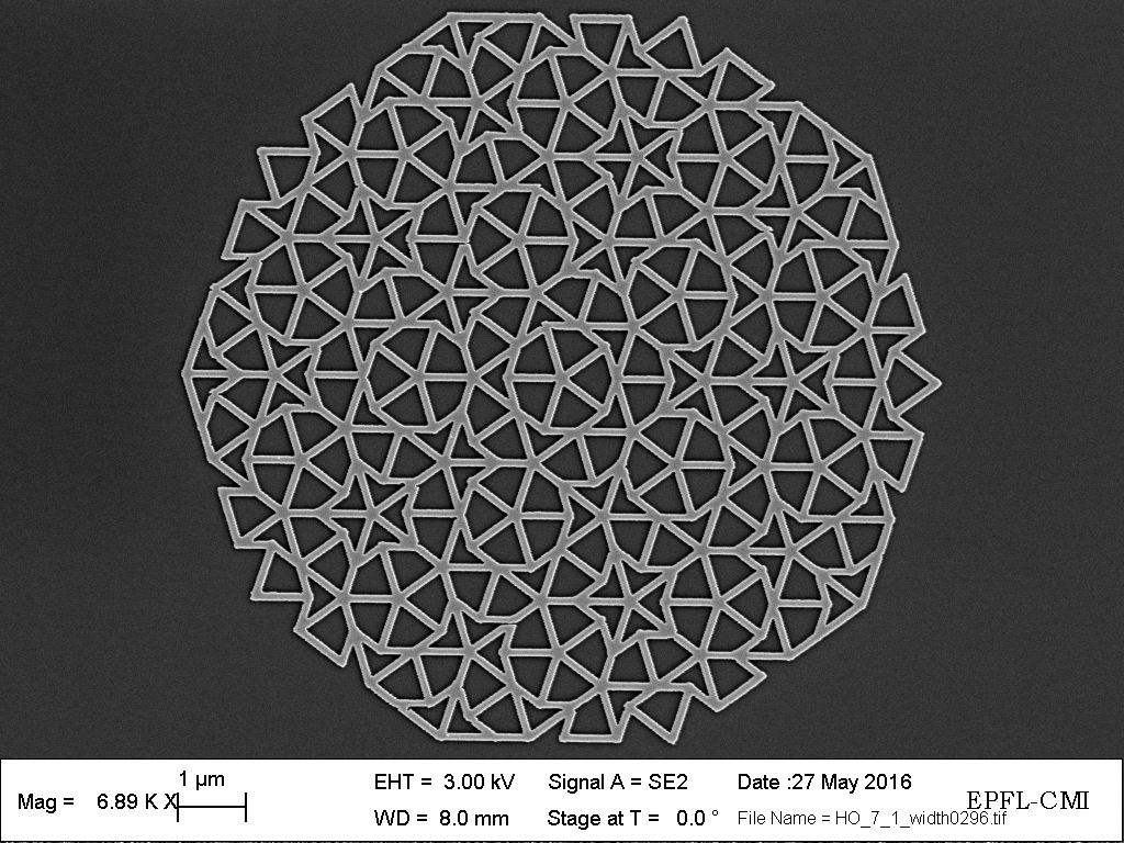
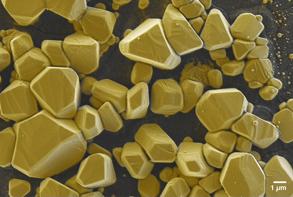
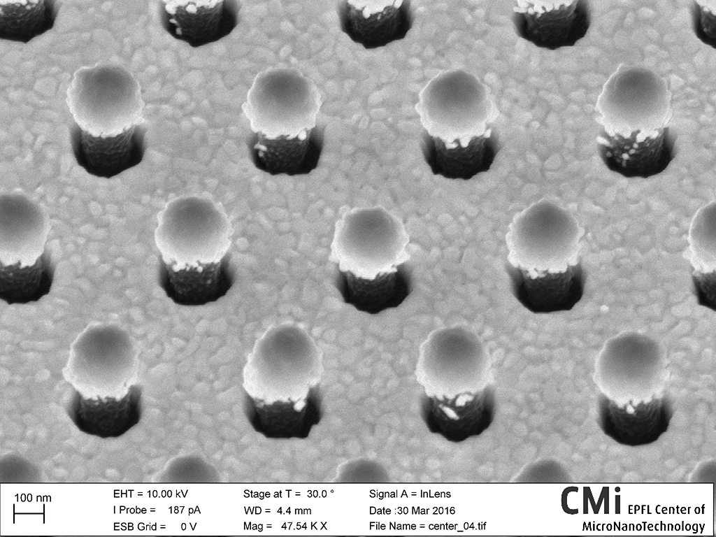
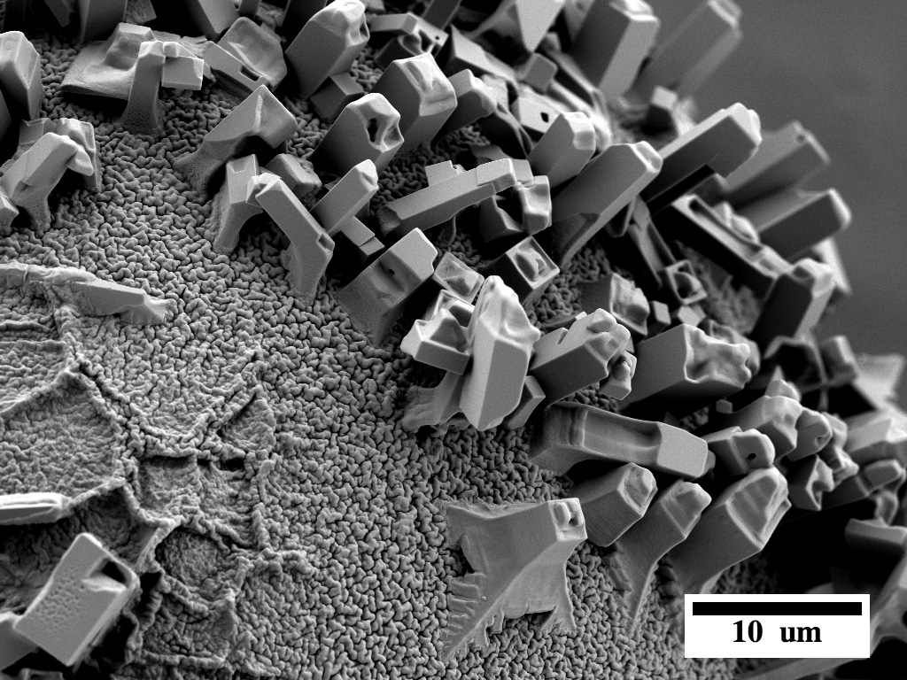
Whole and parts
Jelena Vukajlovic, Wonjong Kim, LMSC
Here is the SEM image of GaAs nanowires on a 4-inch Silicon wafer. After optimizing growth conditions, our tedious SEM session became an enjoyable moment. There are two views on the relationship between the two, which are generally considered to be the whole and the part attached to the whole. 1) The whole is the sum of the simple parts, the assembly, and the thing which is not in the part does not exist in the whole. 2) The whole is more than the sum of parts. What do you think about our nanowires in that sense? We would vote for the latter 😀 (Image was taken in CMi, Zone 15, SEM Merlin).
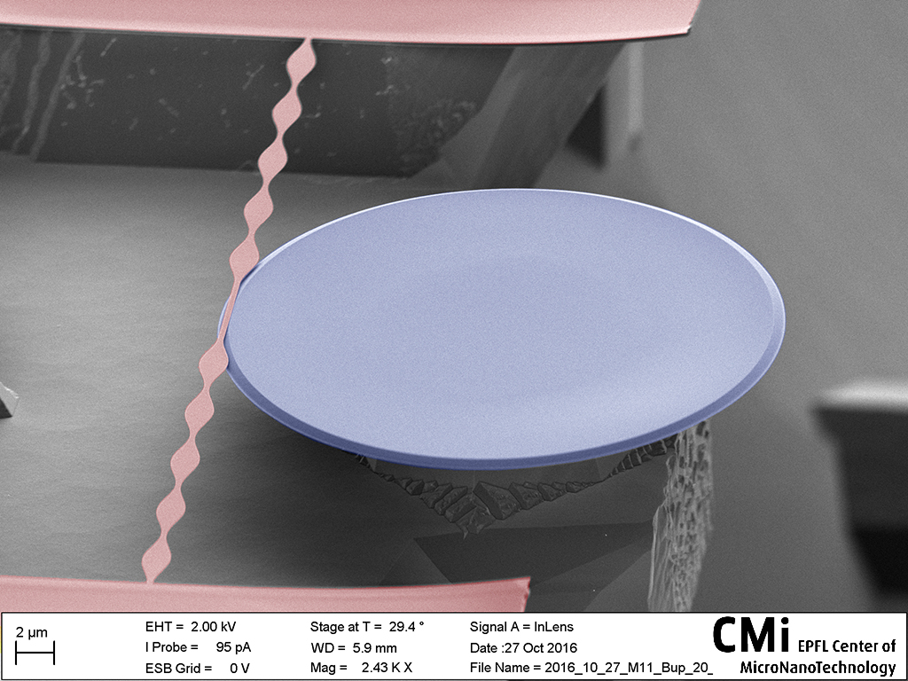
Helping phonons live longer and more productive lives
Ryan Schilling, LPQM
A silicon nitride (red) mechanical resonator is suspended a mere 50 nm from the surface of silicon dioxide (blue) whispering gallery mode optical resonator. The resonators are coupled by radiation pressure, where the beam alters the momentum of photons in the evanescent field of the microdisk. This allows for optical read-out of the beam’s position, with precision orders of magnitude below the standard quantum limit. The beam is designed with acoustic reflectors on either side to focus the energy of a specific vibration to center of the beam, where the interaction with the microdisk occurs. Moreover, the reflectors greatly increase the phonon lifetime over a normal beam, realizing a room-temperature quality factor of 130 000 at 39 MHz. For mechanical sensors thermal force noise fundamentally limits sensitivity to an external force, and in that respect this localization strategy represents a significant improvement over a standard rectangular beam.
Have you ever tried magnifications below one on the SEM?
Marcell Kiss, Q-LAB
Instead of the micro-world, you might just find one like ours! These micro ridges were colorized to show the ‘elevation’: seems like plenty of snow for skiing! This structure was created incidentally on a silicon carrier wafer, which had out-of-focus photoresist patterns and was exposed to chlorine plasma. Image was taken on the LEO and colorized, and all of the processing was done in CMi.
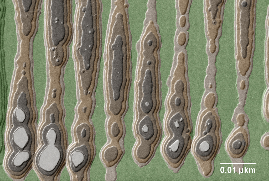
Liberation of the oppressed InAs nanowires: finally they can relax!
Martin Friedl, LMSC
Here we see what happens when strained InAs nanowires (NWs) are grown on top of GaAs nanomembranes via MBE after which the GaAs nanomembranes are selectively etched away. Once the tyrannical GaAs is gone, it stops selfishly imposing its lattice constant (5.65Å) on the poor, stressed InAs NWs and the InAs NWs can relax/elongate to their bulk lattice constant (6.06Å). Since we sputtered down metal contacts before etching (large diagonal bars), the ends of the NWs are fixed. Thus the NWs tend to bow up/down as they relax, marking the beginning of their new stress-free life!
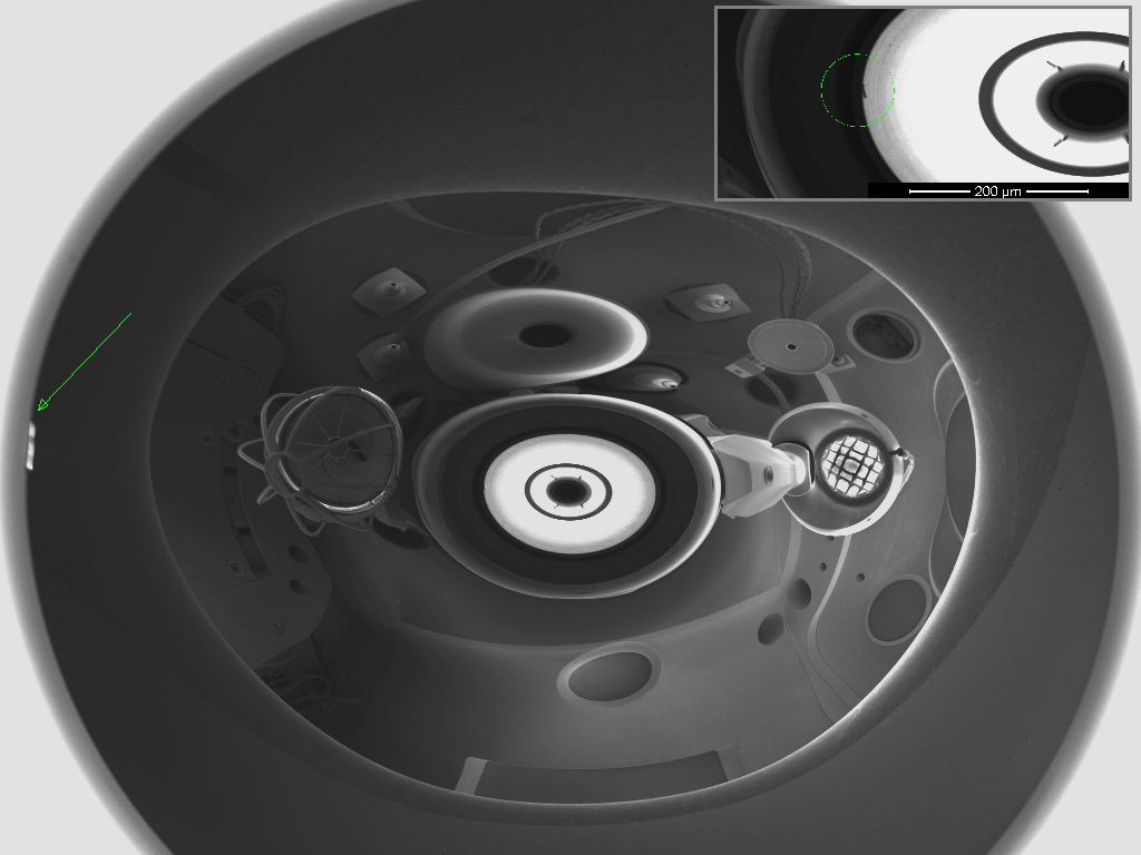
Looking into the mirror!
Joffrey Pernollet, CMI
Attempting to locate the exact position of some kind of residue attached to the pole piece of the SEM column (green arrow on main picture) for proper cleaning and removal, mirror imaging was used to visualize the CMi Dualbeam chamber upside down! A static charge was first build-up on a piece of glass, isolated from ground, by exposing it to a 20kV and 2.4nA electron beam. After a minute, voltage was then switched to 2kV for imaging: the lower potential electrons get repelled from the highly charged surface into the chamber, enabling imaging of all parts inside. Zooming into this “mirror” then allowed for precisely targeting the position of the residue on the left-end side of the pole-piece (circled-out on insert).
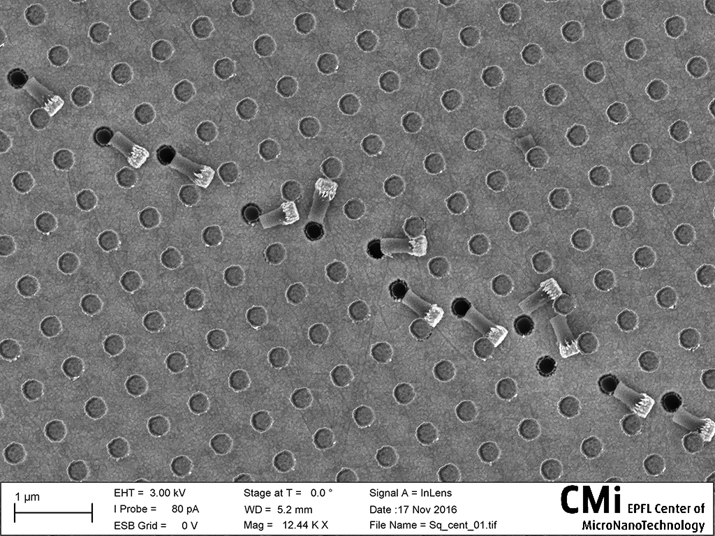
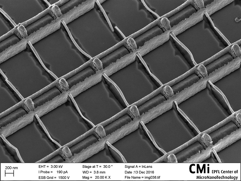
The fallen ones
Cenk Ibrahim Özdemir, BIOS
Handling defects are observed on the arrayed nanopillar resist arrays used for lift-off process.
2016, November
The corset out of thin layers
Jason Jinyu Ruan, Aleva Neurotherapeutics SA
Origami isn’t that easy in a SEM. While trying to fold and shape thin polyimide foils, one might reach interesting results. A thin layer of polyimide is enrolled in a cylindrical shape with its attachment holes on each side. This development is used to make neuro-stimulation electrodes.
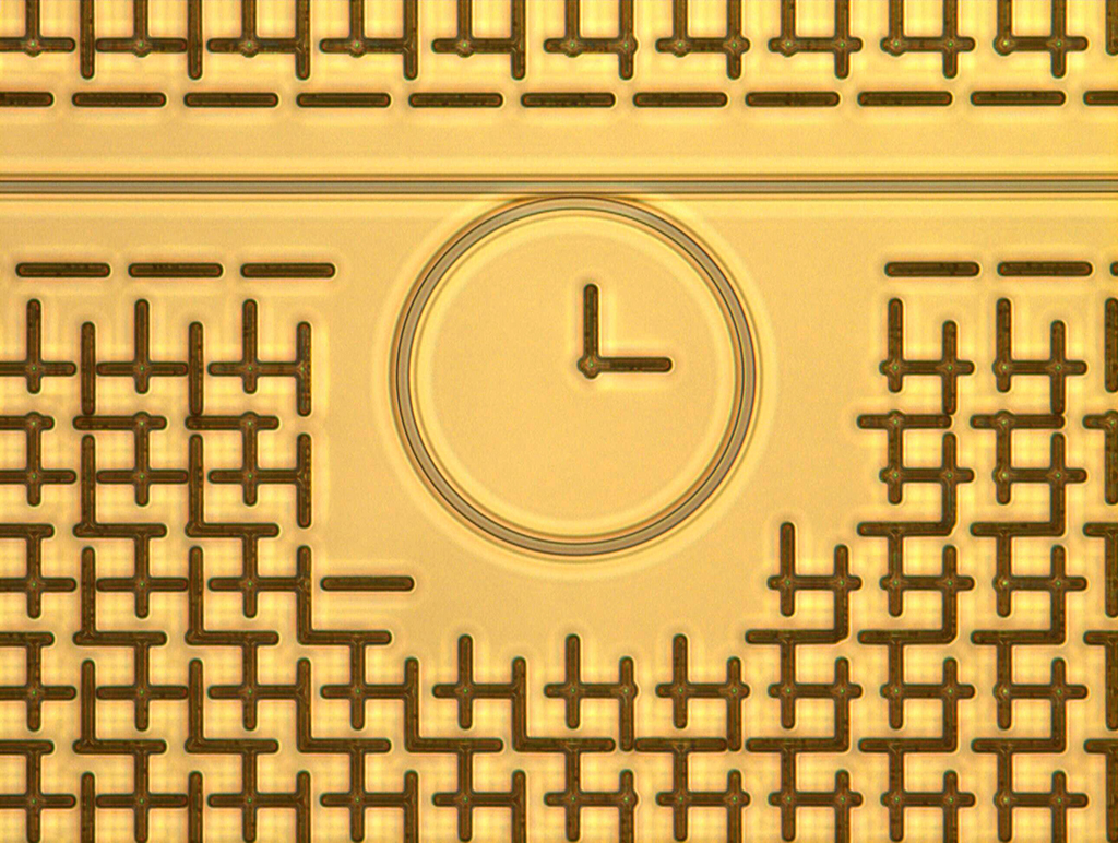
Quarter past 12
Clemens Herkommer, LPQM
This image taken with an optical microscope shows a readily clad microresonator device which is intended to be used for frequency comb generation in the mid-infrared wavelength range. In order to handle the tensile stress of LPCVD-deposited silicon nitride films a stress-release pattern was included to avoid crack formation. During the wafer design the filler pattern is generated with a software routine and sometimes leads to interpretable artefacts, such as a clock showing quarter past 12. Time to go home, for a laborious scientist!
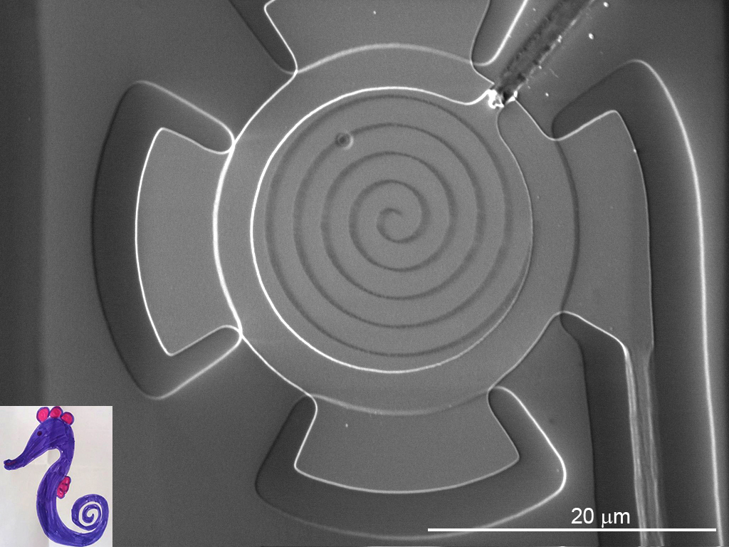
Seahorse’s Tail: The Tale of Listening to Your Own Drum
Sina Khorasani, LPQM
These photos show the successful FIB patterning of a drum capacitor used in quantum electromechanical superconducting circuits. Spiral pattern will help the mechanical resonant frequency to reduce by many orders of magnitude, significant increase in zero point motions, and thus enhancement in single-photon electromechanical interaction rate g0. The reason I would like to call it a seahorse tail follows a painting by my youngest daughter, Atousa 🙂 She has drawn it three months ago at school!
Resist Rainbow
Matthias Neuenschwander, LO
Microelectrodes were fabricated at the CMi. After the strip, some photoresist remained at the edges of the wafer, covering the electrode fingers and creating a pretty colour gradient thanks to thin film interference. Shot with an optical microscope.
2016, October
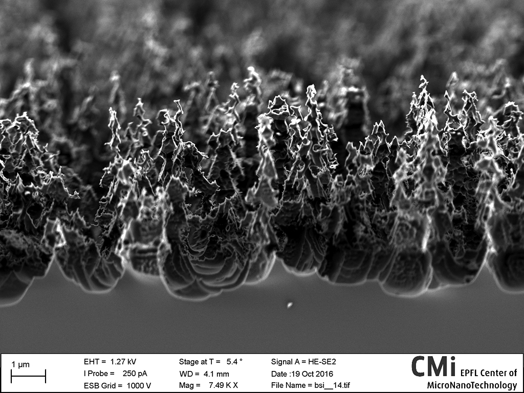
Silicon forest
Niccolo Piacentini, INTEL
Slightly tilted cross-section of a silicon wafer after DRIE-based Black silicon fabrication. The resulting texture resembles to a micro pine forest during winter. Are you willing to get lost among the trees? Equipment: Alcatel 601E. Image: SEM Zeiss Merlin.
Net fishing
Daniel Rodrigo, BIOS
An unidentified species has been trapped by our nanoscale “fishing net”. The image shows in fact a contamination particle trapped under the gold evaporation of a square grid fabricated by lift-off.
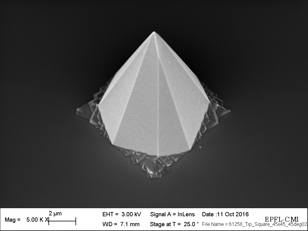
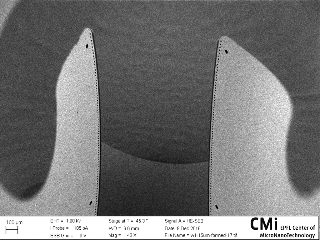
Novel Pyramid Design
Marc Heuschkel, HEPIA – Tissue Engineering Laboratory
The picture shows a protruding silicon tip of 18µm height. The tip has been manufactured by wet chemical etching in KOH 40% using a 200nm SiO2 mask. It is intended as negative master for soft lithography manufacturing of 3D microelectrodes for the monitoring of neuronal tissue in vitro.
2016, September
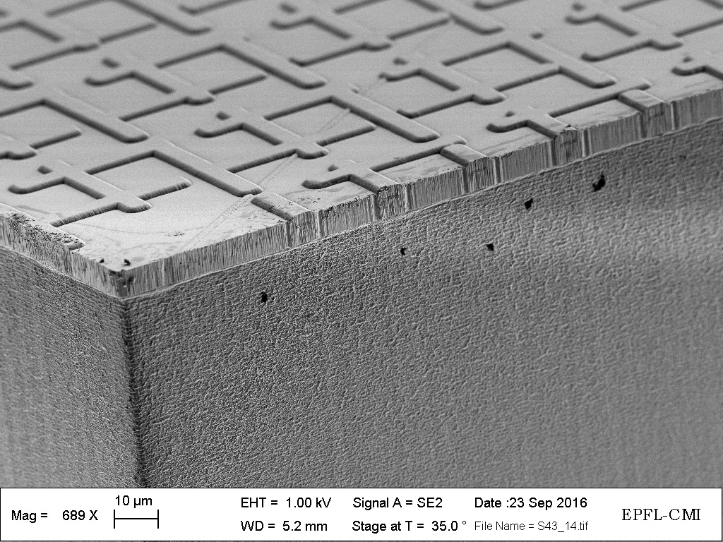
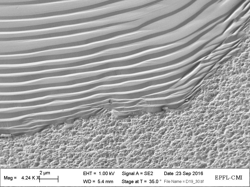
Silicon cliff
Clemens Herkommer, LPQM1
SEM image a silicon-chip facet with oxide layer on top. Photonic circuits are structured on silicon wafers in a >70-step process including: Ebeam lithography, Photolithography, Wet and dry etching, Chemical vapour deposition, Chemical-mechanical polishing. On the picture the signature of Bosch process Si-etching is visible, exhibiting typical roughness as compared to the previous smooth top SiO layer etching.
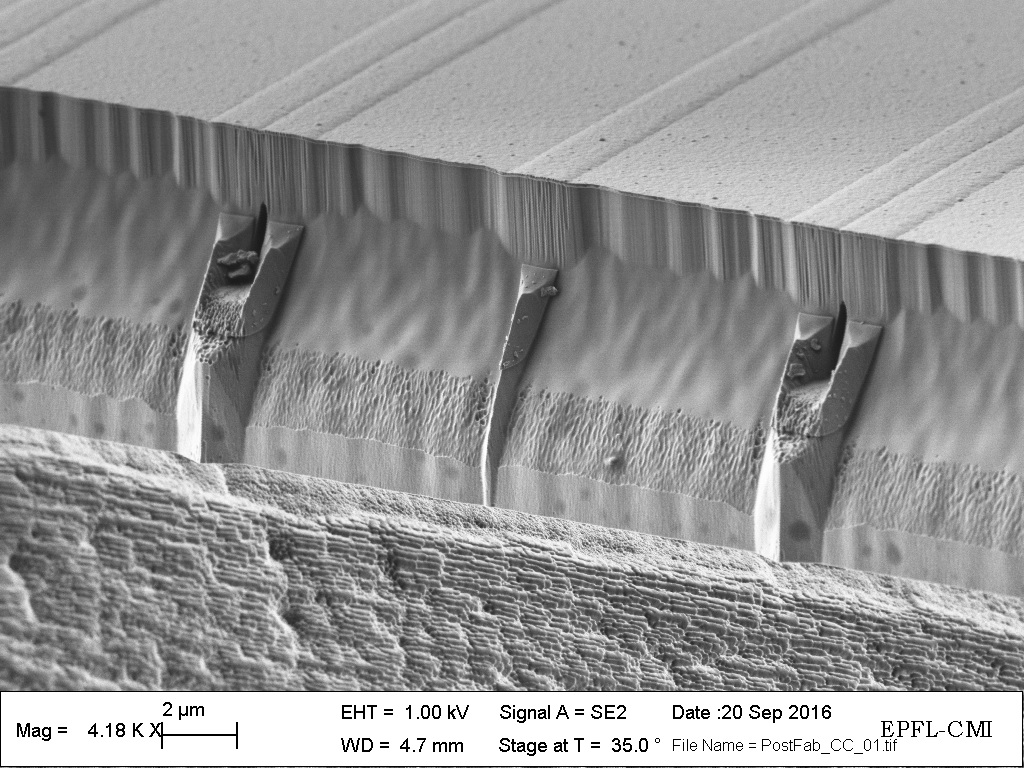
Glass caves
Clemens Herkommer, LPQM1
SEM image of the facet of a silicon-based photonic-circuit chip, showing the end of a silicon nitride waveguide surrounded by two protective structures. The image is taken after a >70-step process, with a run time of several weeks in the CMi clean room facilities. The shown facet was produced by a dry etching step of the SiO cladding to define the facet, followed by Bosch process etching of the silicon substrate. The slanted sidewalls of the oxide cladding are artefacts of burning and swelling photoresist, which was due to insufficient wafer cooling during dry etching.
Fancy LED color controller
Marta Airaghi Leccardi, LNE
Optical micrograph of PDMS dry etching revealing the underlying polymeric layers that produce a color effect. The shiny area at the top is due to the metallic mask.
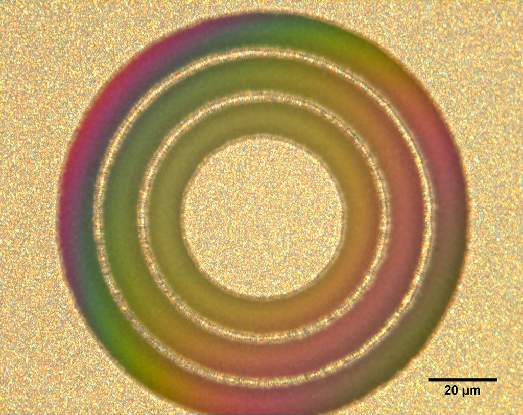
Silicon beach
Clemens Herkommer, LPQM1
SEM image of the surface of a silicon chip, where a flake was broken off during the process of back side grinding. Interference patterns are visible on the surface where the flake broke off, as compared to the rough surface structure produced by deep Bosch process etching. For hard-working scientists the relaxed look at the picture can lead to a brief drifting away and imagination of ocean breeze, waves and a white beach.
2016, August
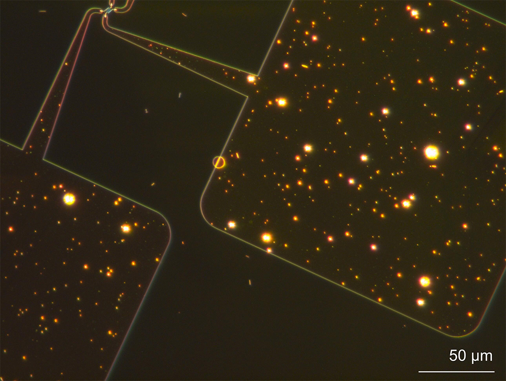
Milky Way, First Contact
Nicholas Morgan, Heidi Potts, LMSC
The galaxy was defined by optical lithography and the stars are spherical gold defects caused by a malfunctioning of the LAB600 evaporation tool. The spaceship in the top left was defined by ebeam lithography. The purpose of this lithography process is to make electrical contacts to InAa nanostructures (too small to be seen). To test our nanostructures, we must land our probes in the Milky Way! The image is a dark field optical micrograph taken in CMi.
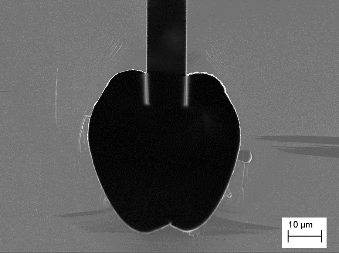
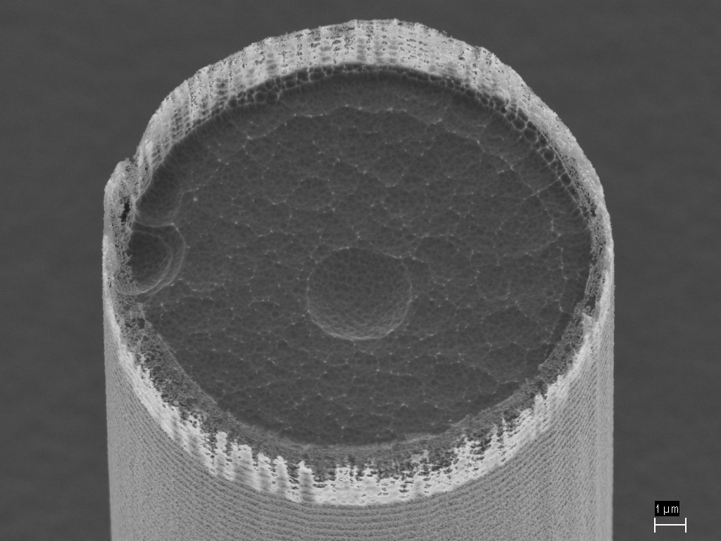
Micro-apple
Dora Fejes-Kajtar, CERN EP-DT-DD
Cross-sectional SEM image of a silicon micro-channel fabricated by using photolithography, plasma etching processes and thin film deposition. The entire sample was prepared in CMi.
Dragon egg
Marco Di Gisi, ANEMS
SEM picture of a gold residue found on silicon dioxide after Cr/Au evaporation.
2016, July

PDMS Labyrinth
Marta Airaghi Leccardi, LNE
The sputtering deposition of a thin metallic layer onto PDMS leads to a non-uniform mask thickness and surface roughness. After PDMS dry etching the pattern is transferred to the substrate and we obtained a… LABYRINTH!
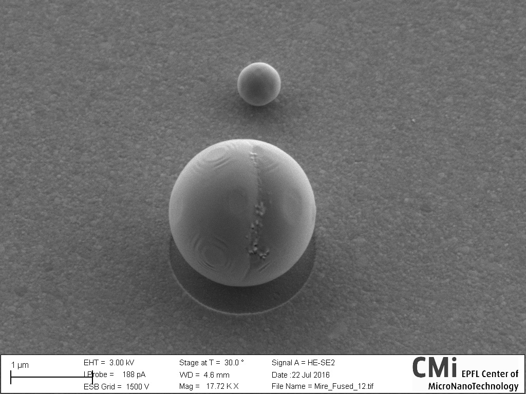
The unwanted golden ones
J. Pernollet, C. Hibert, G. Monteduro CMI
50nm gold coating (evaporation, LAB600H) of a fused silica wafer as a preparation step before ebeam lithography. Even though the wafer was fresh new, Piranha clean and spotless prior to gold coating, the surface then exhibits round sphere-like particles sizing from several tens of nanometers up to few microns. Like visible on the picture, it is interesting to note that some of them masked the coating but others sit on top of the gold layer: it supposes the spheres were continuously created throughout the gold evaporation. EDX analysis seems to confirm this idea: the spheres are made of pure gold.
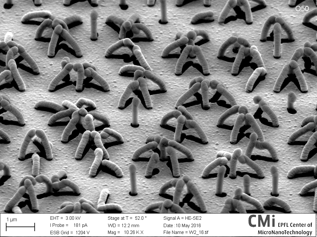
And the bird became a flower…
Benoît Desbiolles, LMIS4
After one day of culture on nano-volcanos array, kidney epithelial cells (HEK) were fixed, dried, and observed with Scanning Electron Microscope (MERLIN). On the figure, salt crystals coming from the cell culture media and mixed of proteins from the cells self-arranged to fake an utopian world. 90% made in CMi.
P.S. The bird starts from the bottom-right corner to end up a flower in the middle left.
2016, June
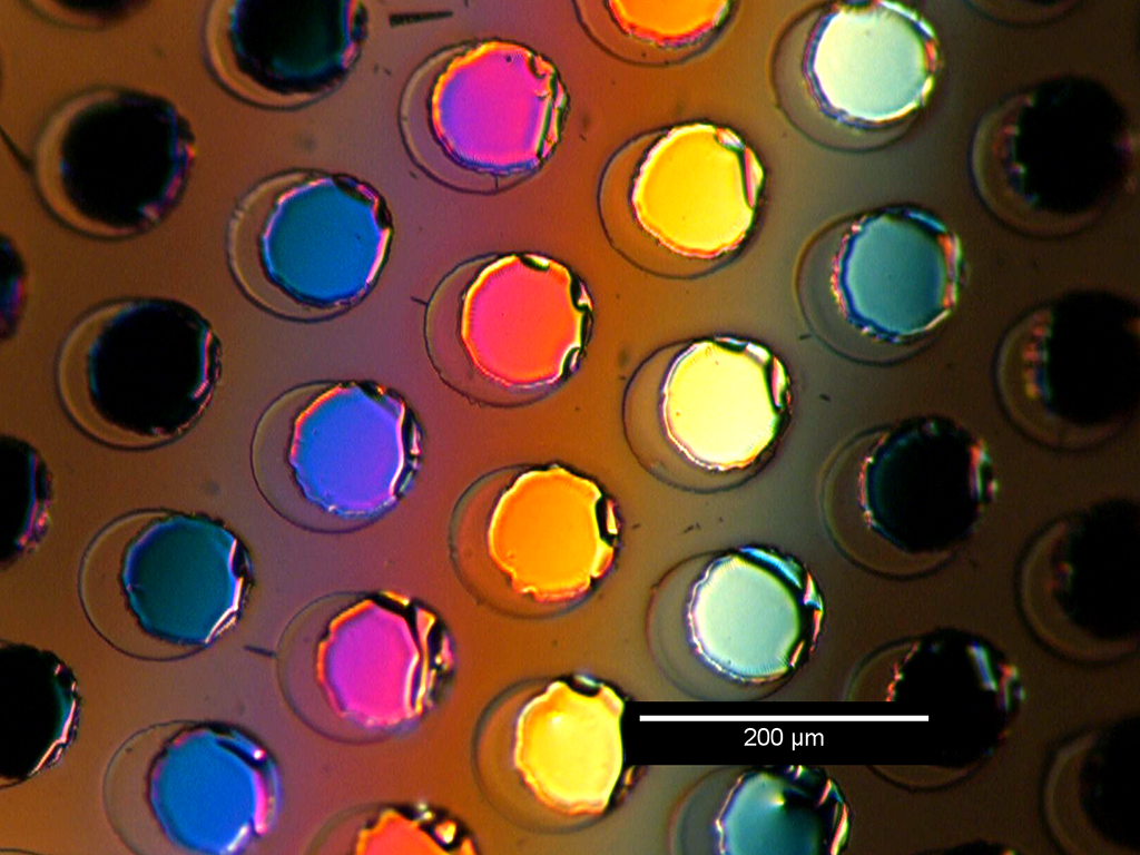
50 shades of light
Marta Airaghi Leccardi, LNE
What we see here is a result of light diffraction on IrOx patterned onto PDMS. The sample was released from the wafer and placed curved under the optical microscope, therefore the individual spots were tilted with different angles, reflecting the light at different colors. (Only contrast was slightly adjusted in post-processing!)
Friday afternoon
Stefano Varricchio, LMIS4
Silicon nanopillars array surfacing from a silicon oxide matrix. The black stars are not an optical illusion -reward of the week gone by- but voids resulting from the conformal deposition of SiO2 on the nanopillars array. The hilly topography of the insulating SiO2 matrix is recognizable as lightly contrasted veining.
Bubble wrap of a PhD student
Stefano Varricchio, LMIS4
Damn, I’ve popp’d them all! – Array of silicon nanopillars surfacing from a silicon nitride matrix. The “hilly topography” is a result of the residual of the CMP slurry which were transferred into the bulk from the successive IBE etching step. The inset shows the topography of the silicon structures resulting from the different etching speed between silicon and silicon nitride during IBE.
Roof top garden fence
Fatemeh Navaee, LMIS4
To prepare PDMS porous membrane, silicon micro pillars were fabricated using photolithography and etching process in CMi. A tiny part of the wafer didn’t cover completely with photoresist during coating process, which leads to having this garden with fence on top of the tower!
2016, May
Pillars brawl
Stefano Varricchio, LMIS4
Composite silicon and carbon structures are covered with a thin evaporated platinum layer. Due to a surface tension during the drying process, the structures collapse against each other. The evaporated Pt layer defines the shadows on the surface and enhances the roughness of the structures.
Going Beyond Periodic Nanomagnetism I
Vinayak Bhat, LMGN
Connected network of Ni81Fe19 nanobars of 25 nm thickness fabricated via electron beam lithography and lift-off techniques on an eight-fold rotationally symmetric quasicrystal tiling known as the Amman tiling. Bright (dark) region corresponds to magnetic (non-magnetic) material.
Going Beyond Periodic Nanomagnetism II
Vinayak Bhat, LMGN
Connected network of Ni81Fe19 nanobars fabricated via electron beam lithography and lift-off techniques on a five-fold rotationally symmetric quasicrystal tiling known as the Penrose P2 tiling. Bright (dark) region corresponds to magnetic (non-magnetic) material.
Eyes in the darkness
Axel Hochstetter, LMIS2
Picture shows a cell sorting device, which is pre-separating red blood cells from bigger cells, like leukocytes or already coagulated platelets. The device was done as a PDMS mold from a SU-8 3025 mask on Si, done in the level +1 cleanroom. The original mask has been fabricated in the -1 level of the CMi cleanroom. The image was taken in phase-contrast mode on an inverted Zeiss microscope and shows lots of cells rushing through the pre filter device, their paths disturbed by some air bubbles, which also form the “eyes” in the surrounding darkness.
2016, April
Wheel of GaAs
Martin Friedl, LMSC
Image shows details of the angular dependence of GaAs nanomembrane growth by molecular beam epitaxy (MBE). The substrate is GaAs (111)B covered with 30 nm of PECVD SiO2 patterned by e-beam and reactive ion etching to selectively expose the substrate below. GaAs nanomembranes are then epitaxially grown in an MBE reactor from elemental precursors. In this top-down image we see how single crystal, defect-free GaAs membranes grow thin and vertical in only three specific crystalline directions on the GaAs substrate. Other directions of growth on the substrate lead to angled and defective membranes. These structures are being explored for their feasibility in various electronic and optoelectronic applications.
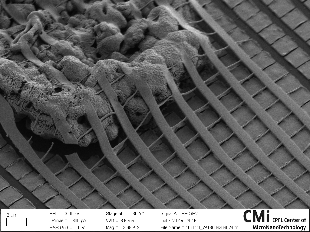
The lonesome nomad
Benoît Desbiolles, LMIS4
Valentin Flauraud, LMIS1
With the lack of adhesion layers a sputtered tungsten film (DP650) delaminated from the substrate creating this desert-like landscape. The sample was cleaved and imaged close to grazing incidence. The debris from the sample SEM preparation resulted in this lonesome nomad looking for his next bright nanoidea in the vast nanoworld. Fake colors added in post-processing.
Micro-moraine
Hadrien Michaud, LSBI
When evaporating gallium on a PDMS substrate coated with a sputtered gold layer, gallium spreads by diffusing and alloying with the gold layer. The resulting film is composed of a solid AuGa2 phase and a liquid gallium phase [1]. We recently observed that if the liquid gallium is forced out of the film, the solid phase remains on the substrate, just like rocks remain on the bottom of the valley when a glacier is retreating. The remaining structures form a micro-moraine of AuGa2 crystallites on the PDMS substrate. The image acquired using the HE-SE2 detector was colorised using the corresponding EsB detector image as clipping mask for material contrast. [1] Hirsch, Michaud et al., Adv. Mater., 2016
2016, March
Seeing blue
Ian Michael Rousseau, LASPE
The SEM image shows a one-dimensional photonic crystal nanobeam optical resonator for a blue nanolaser. The gallium nitride nanobeam, which is 200 nm wide, 300 nm high, and 7 microns long, is suspended in air between two electrodes over a silicon substrate. The light is confined by total internal reflection in the axial dimensions and by the periodic array of holes in the longitudinal direction. By tapering the hole diameter in the middle of the cavity, blue light can be trapped in a volume roughly 1/2 of one cubic wavelength for several picoseconds. The companion 100x dark field microscope image directly shows scattering of blue light by the holey nanobeam. The goal is to tune the laser wavelength in situ by applying a voltage across the electrodes, bending the nanobeam via the piezoelectric effect.
CleanRoom Space Invaders
Andrea Pisoni, Luka Ciric, LPMC
Focused Ion Beam was employed to cut a lamella out from a layered material and to shape it according the “U” structure. Such configuration allows the simultaneous measurement of the electrical resistivity along the different crystallographic direction of the sample. It represents a very reliable method to estimate the electronic anisotropy of a material relevant for electronic applications. The sample was entirely prepared by the Nova Nanolab FIB at CMI. The final shape of the structure reminds us of one of the shapes used in classic video game space invaders.
CuPt cakes
Stefano Varricchio, LMIS4
Multilayered structure of Platinum/SiO2-LTO. The planarization of LTO reveals the Pt nano-structures buried underneath (bright in the middle).
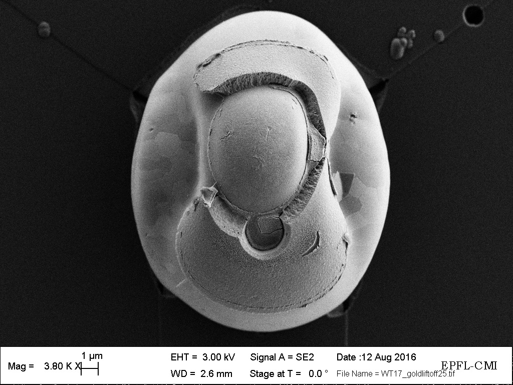
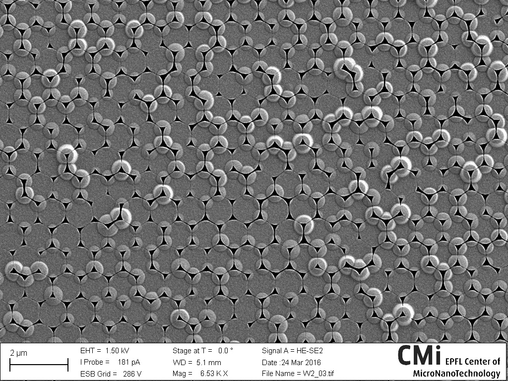
Golden Mushroom Field
Cenk Özdemir, BIOS
Nanopillar array of photoresist is used to obtain nanohole arrays of gold. This SEM image was taken after the gold deposition before the lift-off, showing the mushroom-like gold accumulation on top of the nanopillars. Afterwards, the resist pillars are lifted-off to achieve gold nanohole array structure on the substrate. Nanohole arrays on thin gold films enable plasmonic resonances, which is dependent on the array periodicity, metal type and most importantly, the surrounding dielectric material, which enables biosensing with these plasmonic structures. Optical transmission through a single subwavelength nanohole on a metal film is very limited. But when the nanoholes are well-ordered in an array, they exhibit greatly enhanced transmission with the help of plasmonics, which is the phenomenon called Extraordinary Optical Transmission. Like a well-ordered society accomplishing the extraordinary, isn’t it?
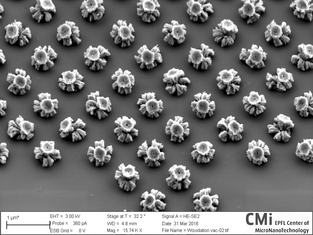
Geranium flowers
Elmira Shahrabi, LSM
These Geranium flowers are made up of tungsten oxide (WOx) in the garden with silicon oxide (SiO2) film soil. This structure shows part of the CMOS 180 nm chip which was post processed in CMI in order to fabricate the Resistive Random Access Memory (ReRAM) co-integrated with CMOS chips. The process flow starts with a photolithography and reactive ion etching (RIE) to remove the top passivation and aluminum metal layers to access the tungsten plugs. Later, the surface of tungsten plugs were oxidized by JETFIRST200 rapid thermal processing (RTP) to form WOx film act as resistance layer in memory.
Bee Nice Today
Stefano Varricchio, LMIS4
Silicon pillars coated with LTO SiO2. During planarization, the void left during SiO2 deposition appears between the structures making it looking like a honeycomb. The production of nano-bees is under development.
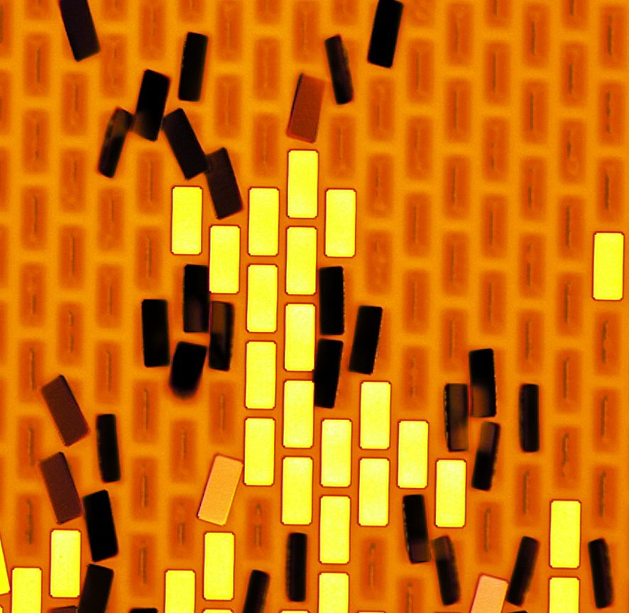
Domino Effect
Yit-shun Leung Ki, Karmic Sarl
Huzzah to springtime, break out the champagne and the Palinka! This is how an etch depth control structure looks when things go right. The domino shaped thin-film mask portions fall as shown when the desired wet etching depth has been achieved. Prior patterning was originally done with the brand new Heidelberg VPG under standard operating conditions and resulting wet etch depth was within 4% of target. The image was taken using the Nikon confocal microscope in Zone 6 with the 20X objective. Image has been cropped and resized in photoshop. COPYRIGHT 2016 Karmic Sarl.
2016, February
Mini City
Huachuan Du, SMAL
The image shows a lot of NaCl crystals located on the surface of hydrogel micro-particle. They resemble the buildings in the city. In the front, there is even a micro Eiffel tower. The sample is made in the PDMS microfluidics fabricated in CMI, the SEM image is taken in CIME.
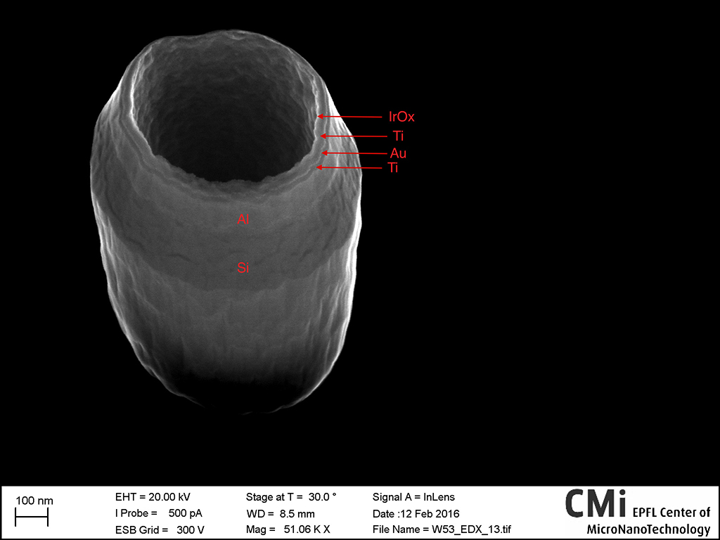
Nano-Volcano
Benoît Desbioles, LMIS4
A wafer coated with several metallic layers is nano-patterned by standard photolithography before to be processed by ion beam etching. The ionic bombardment induces the sputtering of the photoresist side walls, leading to the formation of thin metallic cylinders around the etched platform after resist stripping. Using this method, a 5 nm thin gold ring can be presented on the top of a 600 nm wide volcano. Down into the crater, an Iridium oxide electrode can be used to measure electrical signals from brain cells, with their cellular membrane opened and fused with the functionalized gold nano-ring. 100% Made in CMi.
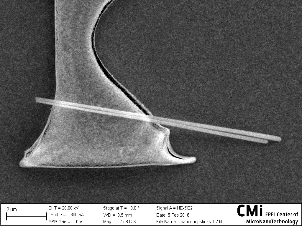
Nano-chopsticks
Natasa Vulic, LMSC
These “nano-chopsticks” are gallium arsenide (GaAs) nanowires grown catalyst-free by molecular beam epitaxy on GaAs (111)B substrates without. Following the growth, the wires are protected from the oxygen (a deep-level impurity in GaAs) by growing a thin arsenic (As) capping layer (~10 nm). This layer is then removed under vacuum conditions prior to growing dielectric films that passivate the dangling bonds on the material surface. Decreased levels of surface impurities that come from the capping of the wires yield better optical and electrical properties since the overall number of trap states that capture the carriers within the GaAs semiconductors are effectively reduced. In the picture, the wires can be seen deposited on a lithographically-defined substrate following ultra-sonication in IPA that removes them from its native substrate, where we can further investigate their optical and electrical properties before and after specific treatments.
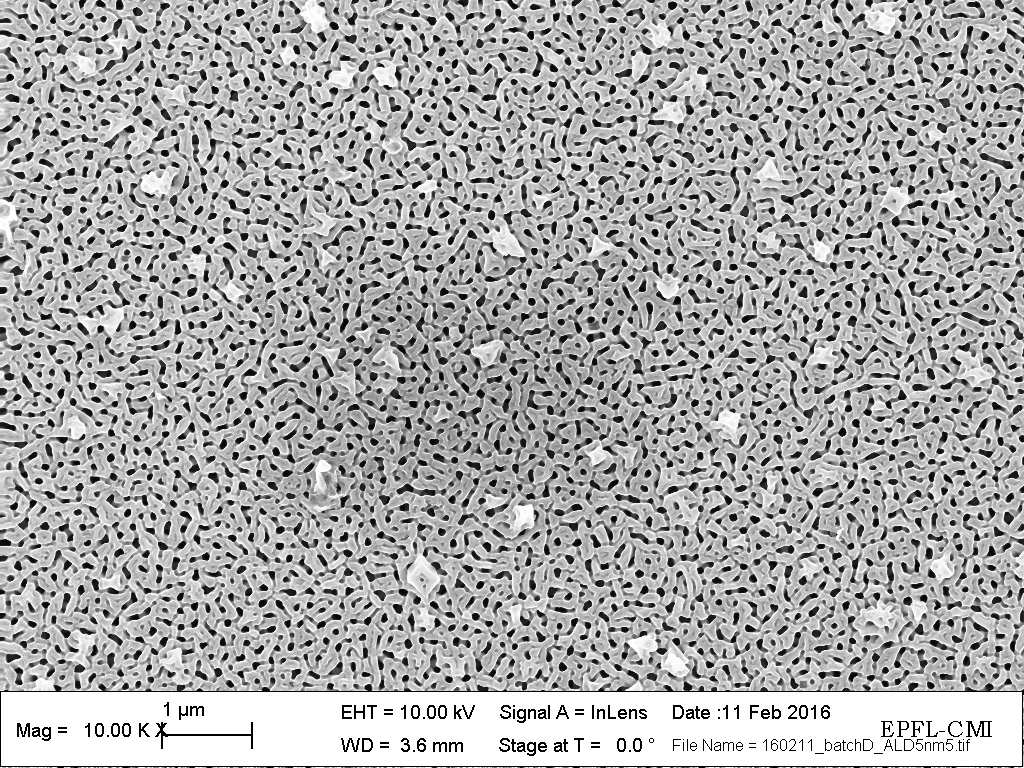
Labyrinth for ants
Carolin Drieschner, LMIS4
Anodized aluminum oxide membrane for cell culture. Due to its high porosity and simple, reproducible fabrication process we are using free-standing aluminum oxide membranes as new biocompatible substrate for intestinal cells from rainbow trout.
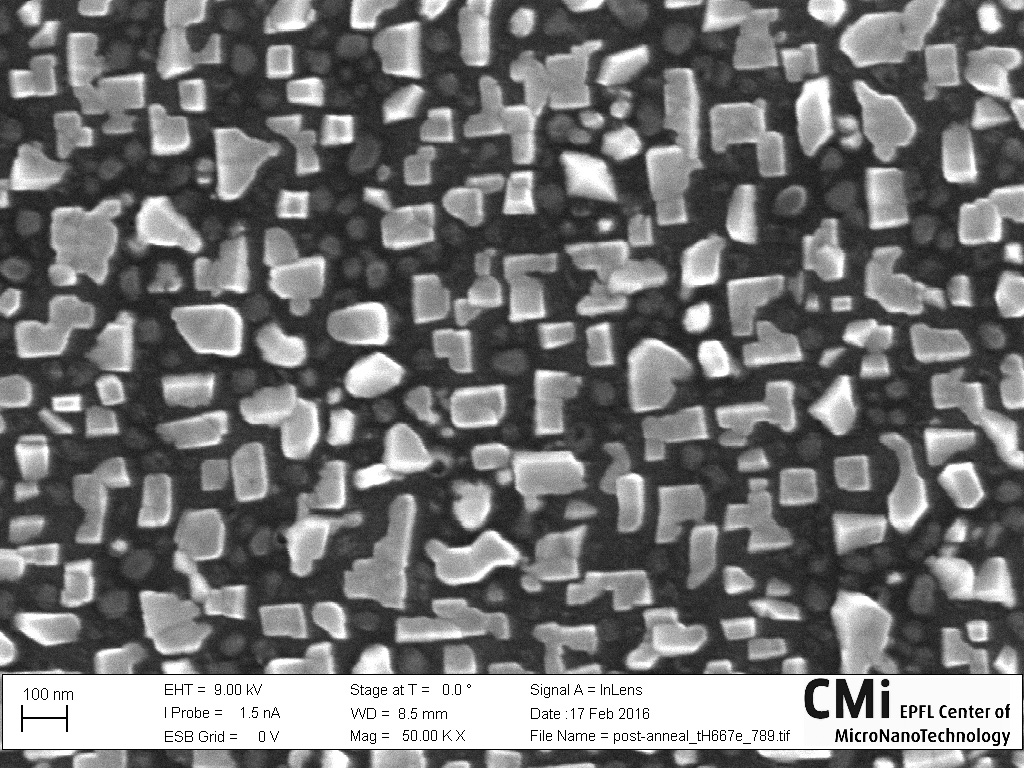
Micro-Tetris
Muriel Blum, MX-PMH, LPMAT
This top-view SEM image shows the microstructure of a barium titanate thin film which was annealed and which has been changed presumably due to the tungsten that was present at certain places on top of the film. Tungsten electrode pads were deposited by sputtering and patterned by photolithography on top of an expitaxial barium titanate thin film deposited by high vacuum chemical vapor deposition on a seed layer of strontium titanate on silicon. Later, the sample was annealed at 600°C under oxygen in order to eliminate the oxygen vacancies in barium titanate. The image was taken at a place between the tungsten electrode pads.
2016, January
Nanobeam & Microdisk
Ryan Schilling, LPQM1
A silicon nitride nanobeam is suspended 30 nm above the top surface of a silicon dioxide microdisk optical cavity. The thermally driven string-like vibrations of the nanobeam alters the path of photons circulating around the perimeter of the microdisk. The photons accumulate a phase shift from the periodic motion of the beam, and this shift is detected in photons leaving the cavity. From this measurement the position of the nanobeam can be determined with extraordinary precision. Remarkably, it’s possible to resolve the amplitude of motion to a value ten thousand times smaller than that imparted by a single phonon (ie. the quantum ground state). This imprecision corresponds to the radius of a neutron, and is achievable both at room and cryogenic temperatures.
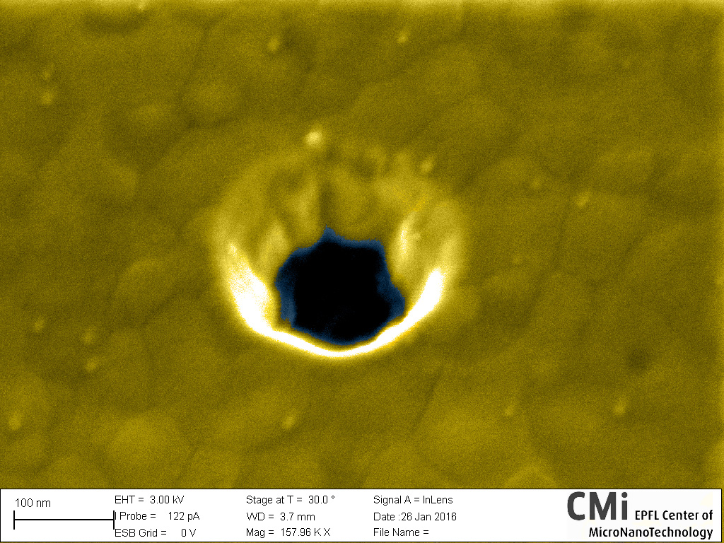
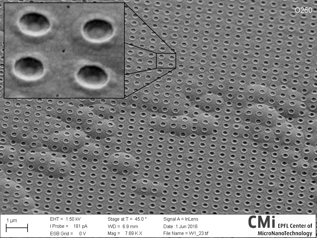
What is in the hole?
Cenk Özdemir, BIOS
What is in the hole? Some stuff for biosensing. This is an SEM image of a single nanohole in a plasmonic nanohole array on gold. Plasmonic nanohole arrays having very high figure-of-merits are used for biosensing with exploitation of extraordinary optical transmission of subwavelength apertures. These gold nanohole array sensors are fabricated with nanofabrication tools at CMi facilities.
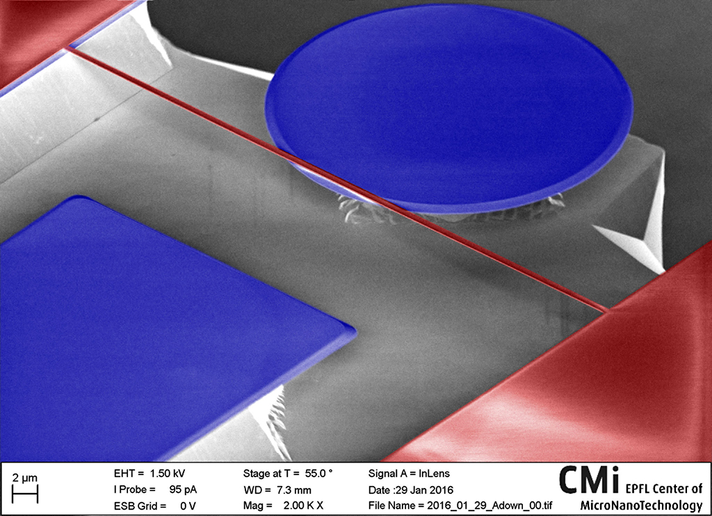
A stronger bond
Pietro Maoddi, Marta Comino, CLSE
It would seem, to the cold and analytical eye of a scientist, that these two SU-8 pillars detached from the substrate during development and were then fused together during the hard bake. However, we like to think that the two of them fell so deeply in love that they decided to break free from the surface – to which they were firmly attached – and ran the 30ųm distance separating them to share a passionate kiss!