Introduction to electron microscopy
Many electron microscopy instruments and techniques are availabe at CIME. They can be divided into three categories: scanning electron microscopy (SEM), transmission electron microscopy (TEM) and focused ion beam (FIB). The next three sections provide an introduction to TEM, SEM and FIB; information on SEM, TEM and FIB techniques can be accessed in the appropriate menus.
Transmission electron microscopy (TEM) uses fast electrons to illuminate a sample. Assuming the sample is sufficiently thin (e.g. 10 – 100 nm thickness), the electrons transmit or penetrate through it. An electromagnetic lens (the objective lens) focuses these transmitted electrons, forming a projected image of the sample. Subsequent electromagnetic lenses magnify the image and project it on to a phosphorescent screen or recording device such as a CCD camera. Compared to light microscopy, the wavelength of the fast electrons is much smaller; for instance, l = 0.00251 nm for 200 keV electrons cf. 400–700 nm for visible light. Therefore a much higher resolution can be obtained compared to light microscopy. Unlike light microscopy, aberrations in the lenses essentially determine the resolution limit of imaging, to values significantly larger than the wavelength of the electrons. Obtainable resolutions for certain instruments in CIME are < 0.2–0.3 nm.
The illumination system uses an electron gun to generate a beam of electrons that is then focused on the sample using condenser lenses. The electron gun consists of an electron source to generate electrons, followed by an anode to accelerate the electrons. The electrons are typically accelerated to energies of 80–300 keV, corresponding to speeds of 0.5–0.8c, where c is the speed of light in vacuum. Electron sources use either thermionic emission from tungsten or LaB6 filaments (i.e. “boiling” electrons off the filament), or field emission, using a strong electric field (109 V m–1) to extract electrons from a metal filament. Field emission guns provide higher brightness (higher current density), better coherence (electrons are more in phase), and a narrower energy spread. The sequence of gun, condenser and imaging lenses form the column of the microscope. A vacuum must be maintained in the column to avoid unwanted scattering of the electrons.
The projected image of the sample is made of contrast determined by the interaction of the electron beam with the sample. Some electrons may be reflected or absorbed – processes that give simple contrast from thickness and atomic number density. However, for thin samples, contrast primarily results from electron scattering by the sample. For instance, atomic planes in crystalline samples elastically scatter (i.e. diffract) the electron beam. This diffraction can be easily seen by projecting the diffraction pattern of the sample on to the screen, or camera, instead of the image. This allows analysis of crystal structure and orientation of the sample. Moreover, imaging using only the direct (“undiffracted”) beam or selected diffracted beam(s) produces key techniques of bright-field and dark-field imaging. A range of other TEM techniques uses these, and other electron beam-sample interactions, to gain access to a wealth of information on the sample.
For good results, TEM requires thin, electron-transparent samples. In general, such samples must also fit the 3 mm diameter disc of the sample holder. Correct specimen preparation to achieve such samples is therefore critical to successful imaging and analysis.
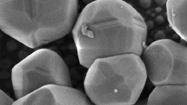
In scanning electron microscopy (SEM), an electron beam is focused in to a small probe and scanned in a raster pattern across the surface of a sample. The electron beam interacts with the sample, generating different signals. By detecting these signals, and correlating signal intensity with probe position, images of the sample surface are generated. The nature of the image depends on the type of signal collected. The most commonly detected signals are: secondary electrons for imaging surface morphology; backscattered electrons for compositional imaging; and X-rays for compositional analysis. Other SEM techniques available at CIME are found here.
As for TEM, the beam is generated by an electron gun. However, much lower energy electrons are used, typically between 1–30 keV. Electromagnetic condenser lenses demagnify the electron source in to a small probe. The probe is focused on the sample surface by a final (objective) lens; this probe is rastered on the sample by scan coils or bobbins. Minimum probe sizes for instruments at CIME are ~1.1–2 nm. However, probe size is strongly dependent on microscope optics, and operating conditions such as beam voltage.
Image magnification is simply determined by the size of raster or scanned area. Image resolution is more complex to determine. While the size of the focused electron probe is important, other factors must also be considered. In particular, different signals (secondary electrons, backscattered electrons, X-rays) come from different interaction volumes in the sample surface. These interaction volumes in turn depend on beam energy and sample composition, and, for backscattered electrons and X-rays, normally result in a spatial resolution much lower than that expected for probe size. For secondary-electron imaging of surface structures, optimal image resolution may not be for the smallest possible probe size, but for the lowest useable beam voltage.
The narrowly converged beam of the electron probe has a high depth of focus. Therefore, unlike light microscopy, very rough surfaces can be imaged. Inherent “shadowing” effects of secondary-electron collection by the standard Everhart-Thornley detector gives images of surface morphology that are readily interpretable. As with image resolution, depth of focus depends on a number of operating parameters. Appreciation of all these factors and imaging modes is therefore critical to obtaining optimal SEM results.
Samples can be bulk pieces of material. While typical maximum samples sizes are a diameter of 10–15 cm, and maximum depth of ~5 cm, the majority of users fit samples on to aluminium stubs of 1 cm diameter. The samples are inserted in to a vacuum chamber; the vacuum conditions mean that samples must not be liquid (apart from for environmental SEM instruments). Biological samples may therefore require dehydration or resin embedding. The electron probe channels a current on to the sample, which must be conducted away to prevent charge accumulation on the sample surface. Samples must therefore be conductive. Non-conductive samples can be made conductive by coating them with carbon or metallic films. Polishing of sample cross-sections can also be crucial to successful compositional imaging and analysis using backscattered electrons and X-rays, and crystallographic analysis using electron backscattered diffration (EBSD) patterns.
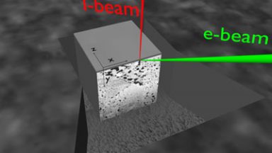
FIB stands for Focus Ion Beam. This microscope works on the SEM principle. But instead of using an electron beam, it uses an ion beam, usually gallium ion. It can be used as a normal imaging microscope, detecting either secondary electrons either secondary ions. Compare to electrons, ions have higher mass and higher momentum. Thus when interacting with a sample, ions modify it by implantation or by sputtering. Moreover a gas precursor can react under the ion beam depositing a material.
Coupled with a SEM to form a dual beam station, the FIB becomes a powerful tool for material science and life science. In the microscopic field, three techniques using FIB dual beam can be highlighted: TEM lamella preparation, cross section and tomography.