Secondary-electron (SE) imaging
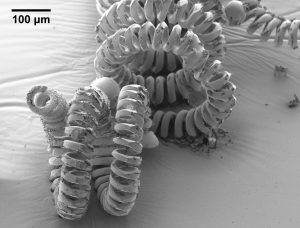
Inelastic scattering of the electron beam leads to ejection of secondary electrons from atoms in the sample. Because of their low energy (e.g. < 50 eV), only secondary electrons from within a few nanometres of the surface can escape from the sample and hence be detected. Secondary-electron (SE) detectors measure the intensity of SE emission as the electron beam rasters across the sample, for instance by using a small voltage bias to attract the SE electrons to a scintillator-photomultiplier system, as with the classic Everhart-Thornley detector. The large depth of field of SEM imaging, combined with the surface nature of SE emission, produces images with excellent definition of the surface morphology and topography of the sample. Further, effects such as greater SE escape from corners that renders edges sharp, and inherent shadowing from three-dimensional objects, are often analogous to the interaction of macroscopic objects with ambient light. As a results, SE images are readily interpretable by the human eye. This ease makes the technique a straightforward but powerful way of interpreting the micro- and nano-scales.