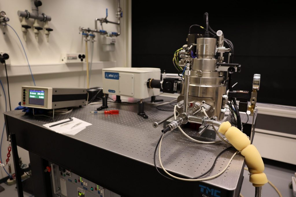
The Attolight Allalin (Rosa 4634) is a dedicated SEM that implements cathodoluminescence (CL) detection as a reflective microscopy objective embedded within the pole piece. This allows for CL acquisitions to encompass large areas without loss of signal.
Microscope design and optics
In the schematics of the electron microscope column with the CL detection optics: Electrons from the electron gun (green tip and two rings at the top) are collimated by the gun lens and then focused by the Objective Lens on the sample (red slab). The CL objective and tilted mirror ensemble, embedded into the objective lens, gathers the CL signal and focuses it into the spectrometer, depicted as two parabolic mirrors and a diffraction grating. The signal can be directed on two different detectors by a motorized plane mirror: a CCD for near UV-Visible light (250-950 nm) detection, and an InGaAs photodiodes array (PDA) for the detection of near Infrared (NIR 1000-1700 nm) signal.
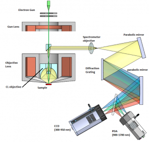
Schematics: Attolight commercials
Schematics of the CL microscope with electron and light optics, electron beam (green) and CL signal (yellow/rainbow). Not shown on the schematics is the beam aperture, located between the two electron lenses, which allows to align the beam in the column and control the beam current together with the gun lens.
Basic specification
|
Instrument |
|
|
Beam Energy |
1-10 kV |
|
Probe Current |
100 pA – 20 nA |
|
Sample Temperature |
5 – 300 K |
|
Spatial Resolution |
5 nm |
|
Max. Sample Thickness |
2.5 mm |
|
Spectroscopy |
|
|
CL objective Numerical aperture |
0.71 (f/0.5) |
|
Detection range |
200 nm – 1700 nm |
|
Spectral resolution |
0.37 nm |
List of Publications
Concept of Cathodoluminescence
Cathodoluminescence Spectroscopy (CL) is a luminescence measurement technique where an electron beam impinging is used to excite a sample, giving raise to emission of light (UV-VIS range) that can be then detected and analysed. Like X-ray spectroscopy, Electron-Beam-Induced-Current, Secondary-Electron Emission, it is a secondary signal present in Scanning Electron Microscopy and can thus be used as a SEM imaging technique.
Similarly to Photoluminescence (PL), CL can provide precious functional informations on electronic materials properties such as band-gap, defects and impurities. However, because the electron beam can be focused to a nanometric spot on the samples, the spatial resolution of CL maps are unmatched. In addition to this, large band-gap semiconductors can be studied because energetic electrons can easily provide several eV’s of energy to the sample, in the range where deep-UV lasers are not readily available and/or very expensive.