This research is part of the nano-tera.ch project Platform Circuit Technology Underlying Heterogeneous Nano and Tera Systems (PlaCiTUS).
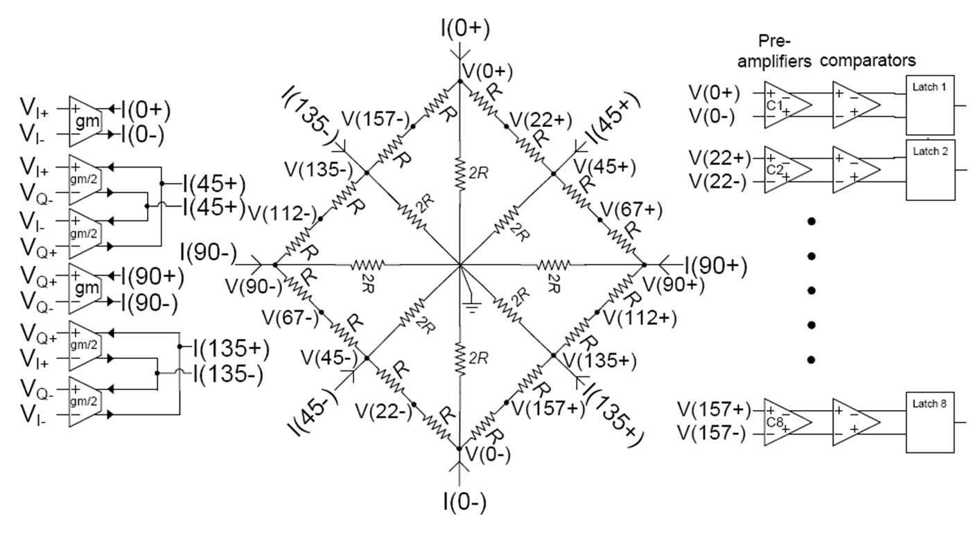 |
| 4-bit Phase ADC schematic |
Many wireless communication systems employ constant envelope modulation schemes which contain the signal information in the phase. But traditional wireless systems instead of directly exploiting this phase information extract the amplitude information in the I and Q domain separately using amplitude ADCs to recover the signal information. A phase ADC on the other hand works on the principle of converting the actual phase between the I/Q signals directly using a linear network into a digital representation of the position of the rotating phasor in the constellation diagram. The basic idea of the phase ADC is that the addition of two sine waves give rise to another sine wave with a phase shift. In a phase ADC this is achieved by feeding the two signals which are in quadrature (the recovered I and Q parts of the phase modulated signal) to a linear resistive network. The generated sine waves at the various nodes of this linear network can then be fed into a detector which detects the zero crossings to generate a circular thermometer code of the quantified phase. The fundamental advantage of such a phase ADC is that it does not need any absolute reference voltage to do the phase quantization since the quantization principle is based on relative phase information. Since no reference voltage is needed the number of comparators needed is halved as compared to traditional amplitude domain ADCs for the same bit resolution. In its operation the minimum signal it can handle is limited only by the noise of the circuit along with the offset voltages of its constituent blocks while the maximum signal it can handle is limited by the linearity of the circuit. Consequently it has the potential to provide a higher dynamic range as compared to traditional amplitude ADCs.
A 4-bit phase ADC was implemented as part of the transceiver SoC integrated in a 0.18 μm standard digital CMOS technology. With a supply voltage of 1.25V, the current consumption was found to be 290 μA while with a supply voltage of 1.7V the current consumption was measured as 310μA. From the measurements it is found that the maximum signal for which there is half LSB phase quantization error in one of the codes is 806mV while the corresponding minimum value is measured to be 7.1mV. So from this measured values the dynamic range can be calculated to be 20 log(806/7.1) = 41.1dB. This dynamic range is independent of the supply voltage. To achieve a similar dynamic range a traditional amplitude domain ADC will need 7 bits. This will necessitate 8 times more comparators and resistors which in turn means more chip area and an increased power consumption by the same factor.