Motivation
The Large Hadron Collider (LHC) at CERN is the world’s largest and most powerful scientific facility ever built. It had discovered the long-sought Higgs Boson in 2012. To promote the scientific progress, it will need a major upgrade around 2020 for a higher luminosity. The HL-LHC will rely on a number of key innovative technologies including much more radiation-tolerant silicon tracking systems with higher granularity and higher bandwidth. In particular, the pixel detectors closest to the collision points will reach an unprecedented radiation level of 1 Grad of total ionizing dose and 1016 neutrons/cm2 over 10 years.
Transistors with a thinner gate oxide demonstrate a higher radiation tolerance and bulk CMOS technologies seem to be more radiation-tolerant than SOI technologies. Therefore, we propose to investigate the use of a 28 nm bulk CMOS process for both a higher radiation tolerance and higher bandwidth. However, since 45 nm technology node, a bilayer gate dielectric composed of a thin high-k material and an interfacial silicon dioxide has been introduced. In addition, the shallow trench isolation oxide is still in the order of 100 nm. The effects of the charge buildup related to the bilayer gate oxide and the STI oxide remain unclear in deep submicron MOSFETs.
Objective
The objective of this project is to understand and accurately model the effect of cumulated dose on MOSFETs using the industry-standard BSIM6 compact MOSFET model that would enable designers to design circuits while accounting for the impact of cumulated dose on device behaviors. In addition to the obvious impact on the threshold voltage, the carrier mobility, and the subthreshold swing, cumulated dose certainly has an impact on the noise of the device, particularly the flicker noise. To this end, the impact of cumulated dose on all aspects of the device operation will be investigated and modeled in BSIM6, which can then be directly used by the circuit designers.
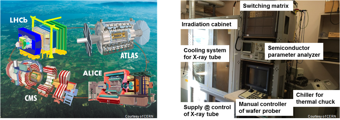
Results
Measurements have been conducted on 28 nm bulk MOSFETs at a varying total dose up to 1 Grad. We have observed the effects of total dose on the threshold voltage, the carrier mobility and the slope factor as well as on the drain-to-source leakage current [1-3]. These allow us to continuously develop both physics-based and compact models for DC, CV and noise performance of MOS transistors at harsh radiation environments.
[1] A. Pezzotta, C. M. Zhang, F. Jazaeri, C. Bruschini, G. Borghello, F. Faccio, et al., “Impact of GigaRad Ionizing Dose on 28 nm bulk MOSFETs for future HL-LHC,” in 2016 46th European Solid-State Device Research Conference (ESSDERC), 2016, pp. 146-149.
[2] C.-M. Zhang, F. Jazaeri, A. Pezzotta, C. Bruschini, G. Borghello, F. Faccio, et al., “GigaRad Total Ionizing Dose and Post-Irradiation Effects on 28 nm Bulk MOSFETs,” in 2016 IEEE Nuclear Science Symposium Conference Record, Strasbourg, 2016.
[3] C. M. Zhang, F. Jazaeri, A. Pezzotta, C. Bruschini, G. Borghello, F. Faccio, et al., “Characterization of GigaRad Total Ionizing Dose and Annealing Effects on 28 nm Bulk MOSFETs,” IEEE Transactions on Nuclear Science, vol. PP, pp. 1-1, 2017.
[4] C.-M. Zhang, F. Jazaeri, A. Pezzotta, C. Bruschini, G. Borghello, S. Mattiazzo, et al., “Total Ionizing Dose Effects on Analog Performance of 28 nm Bulk MOSFETs,” in 2017 47th European Solid-State Device Research Conference (ESSDERC), 2017.