Motivation
Advanced Systems-on-Chip (SoCs) consist of millions of devices with the MOS transistor being the key element among them. The widely recongized advantages of CMOS resulted in it becoming the leading technology for microelectronics industry. Modern CMOS devices have scaled down to unprecedented levels – today ~20 nm and they are expected to scale even further in the next few years. The aggressive downscaling along with the innovative techniques applied in deep-submicron CMOS technologies have brought into play several questions regarding the behavior of MOS transistor.
The state-of-the-art downscaled CMOS processes may provide smaller and faster devices, resulting in an increase of the speed and density of SoCs, yet, there are certain applications where reducing the power consumption remains a priority. Design in the sub-threshold region could help towards less power consuming circuits, however characterizing and modeling the behavior of MOSFET at low current densities can be rather challenging, especially when the device operates in RF and also noise is accounted for.
Objectives
- Characterization and analytical modeling of the behavior of advanced nano-scale MOSFETs emphasizing in subthreshold and RF operation, including RF noise.
- Evaluation of state-of-the-art compact models by comparing them against measurements of advanced CMOS technologies. Enhancement of the models so that they can provide a reliable description of nano-scale MOS transistors, for dynamic, static and RF operation, including noise, focusing mainly on low levels of inversion.
Main Results
- We developed simple and straightforward analytical expressions, valid from weak to strong inversion, which can be used during device characterization or circuit design, to predict the RF behavior of MOSFET, including the noise. Furthermore, we established an efficient and straight-forward parameter extraction procedure for the RF and the RF noise model parameters. The analytical expressions were validated against measurements of a commercial state-of-the-art 40 nm CMOS process.
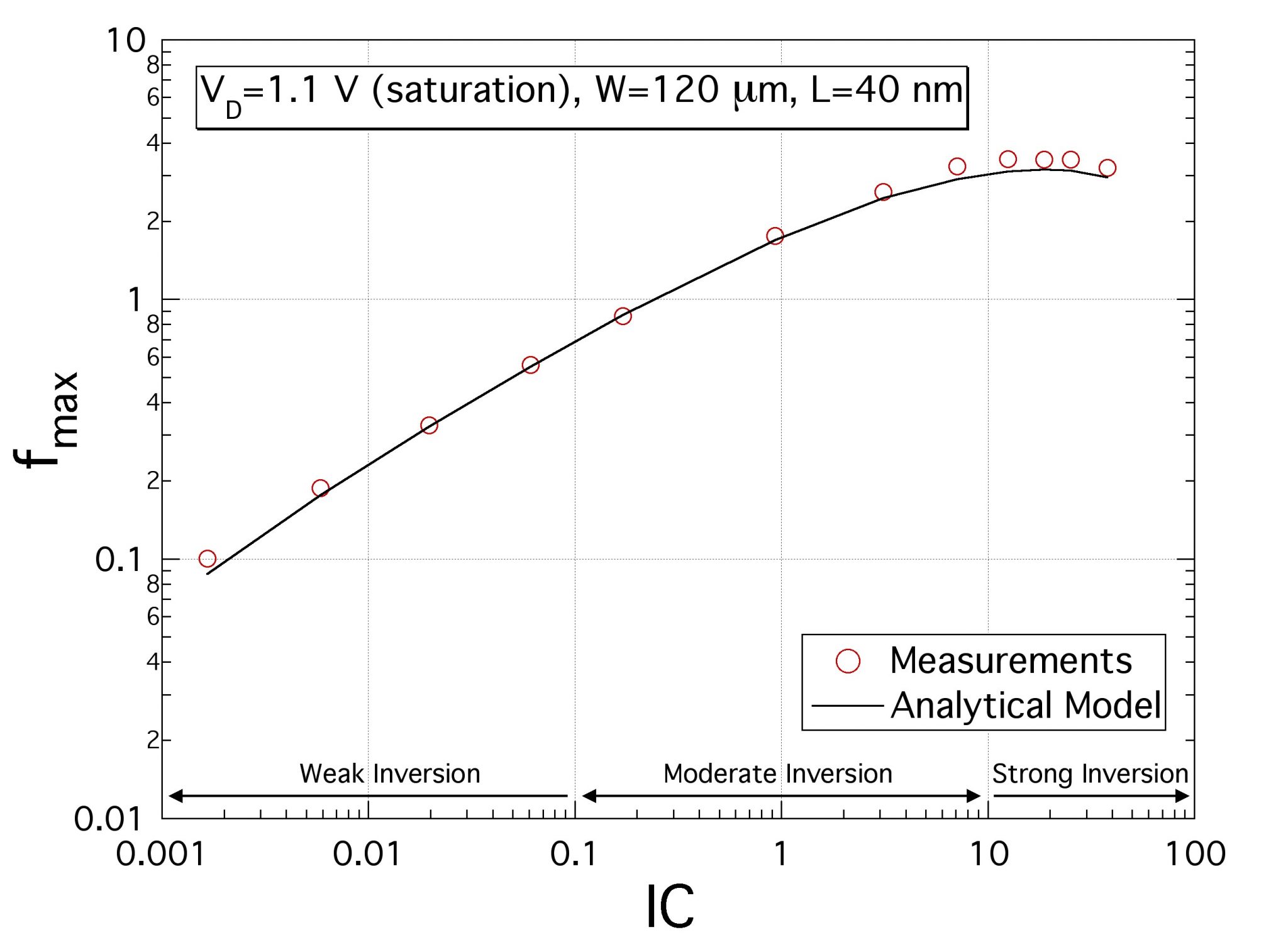
An analytical expression to calculate Fmax, across different levels of inversion, was developed. Above, the normalized Fmax vs. the inversion coefficient (IC) is shown. The analytical model predicts accurately the Fmax of a 40 nm NMOS device, accounting for the different trends in weak and strong inversion.
- In collaboration with the BSIM team in Berkeley on one side and ST Microelectronics (STM) on the other side, we worked on the enhancement and evaluation of the BSIM6 model, with the target to be the next standard model for bulk MOSFET. After an extensive and tough evaluation procedure by the members of the Compact Modeling Coalition (CMC), BSIM6 was voted to become the next industry standard in April 2013.
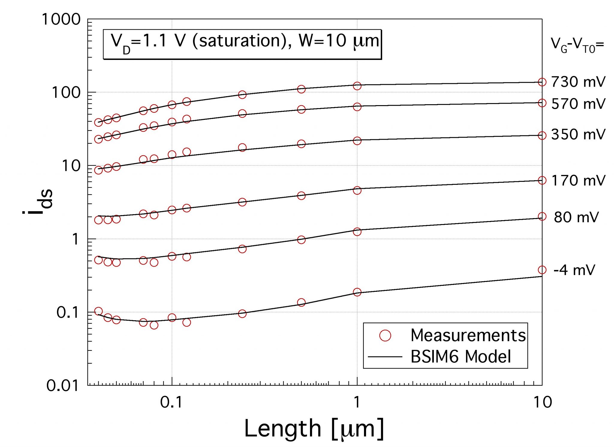
The equations for width/length scaling in BSIM6 were developed at EPFL. In the above plot, the normalized drain current across length, from weak to strong inversion, is shown. The model is compared against measurements of a 40 nm CMOS process. The good scalability of the model is demonstrated.