Background
Even with today’s best supercomputers, some problems remain practically impossible to solve. Their time to solution grows exponentially with the problem size. Two examples are optimization problems subject to many constraints and the study of complex quantum systems. In these cases, one settles for sub-optimal, approximate solutions or finds no solution at all. Solving them would have a big impact in any aspect of society, whether in health (finding new medicines), logistics (optimizing distribution routes) or in currently unimaginable ways by understanding the evolution of complex quantum systems.
Quantum systems contain exponentially more information when the system grows. The idea behind building a quantum computer is to use this fact to solve exponentially growing problems. A quantum computer relies on a new processing core for the computer, based on quantum bits (”qubits”) storing the information in entanglements between different qubits.
Challenge
The qubit entanglements are very fragile. The slightest fluctuation in the material or disturbance from outside can easily de-entangle the qubits. The qubits will then start acting like normal bits once again, making the quantum computer lose all its additional computational power over supercomputers. To keep this qubit decoherence at a minimum, the qubits are operated at cryogenic temperatures, which brings at least the thermal noise as low as possible.
To operate the qubits, a control system is necessary. A bulky control system operated from outside the cryogenic liquid can be too ”noisy” for the qubits. However, all the parts of the control system can also be integrated on a much tinier chip, next to the qubits, in silicon CMOS technology. Such a ”quantum IC” requires that the control system, including its key building block, the MOS transistor, operate at cryogenic temperatures and low power, minimizing the heat dissipation to the qubits.
Project
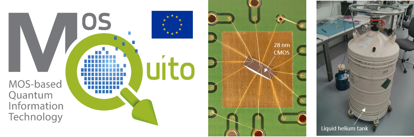
To design these cryogenic control circuits, mainly analog and RF circuits, a full-fledged cryogenic MOS transistor model is essential, in order to meet the specifications at cryogenic temperature and avoid expensive respin of IC fabrication. Developing such a model is ICLAB’s mission within the European H2020 MOS-Quito Project (MOS-based Quantum Information Technology). A 28 nm bulk CMOS technology has been measured and analyzed at liquid helium temperature indicating strong improvements in mobility, subthreshold swing and analog design parameters [1]. These initial results allow continuing the development of both physics-based and compact models for the MOS transistor at cryogenic temperatures, including DC, CV and noise performance.
[1] A. Beckers, F. Jazaeri, A. Ruffino, C. Bruschini, A. Baschirotto, and C. Enz, “Cryogenic Characterization of 28 nm Bulk CMOS Technology for Quantum Computing,” in European Solid-State Device Research Conference (ESSDERC), 2017