|
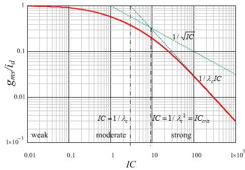
Current efficiency versus inversion coefficient for a short channel device |
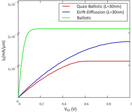 |
| Comparison of ID-VDS characteristics of ballistic, quasi-ballistic and drift-diffusion devices |
Deeply scaled sub-micron technologies have resulted in very high possible operating speeds for RF circuits with transit frequency ft and the maximum frequency of oscillation fmax reaching several hundreds of Gigahertz. However, for an increasing number of applications low power consumption is a more critical issue than high speed operation. Significant power saving can be achieved in RF circuits by shifting the transistors’ operating point from strong inversion towards weak inversion. Yet, shifting the operating point towards weak inversion might not be straightforward in nanoscale technologies. The nanoscale devices are expected to have quasi-ballistic and ballistic transport and stronger short-channel effects. Evidently, nanoscale devices cannot be modeled adequately with conventional approaches. The existing compact models need to be evaluated for nanoscale devices with respect to their ability to model the physical behavior, especially in weak-inversion, and eventually new models could be needed.
The main objectives of this project are:
- Fully characterize several nanoscale CMOS technologies (65 nm or 45 nm, depending on availability, and then 32 nm) for operation in weak inversion for analog and RF circuits. The characterization includes dc, small-signal, RF and noise parameters.
- Evaluate the behavior of existing compact models in weak inversion by comparing with measurements. Improve the models by including ballistic regime in a continuous way, and derive a clear design methodology in order to be able to efficiently design analog and RF circuits operating in weak inversion and integrated in nanoscale technologies.
- Evaluate the improved compact models together with the design methodology through the design of simple but representative analog and RF building blocks.