Background
An optimum design means the best trade-off between several aspects, usually represented by gain, current efficiency, bandwidth, linearity and noise performance. To achieve this, designers often start using simple transistor models before fine-tuning with the design-kit. However, this task has been made more difficult in advanced CMOS technologies due to the down-scaling of CMOS processes and the reduction of the supply voltage, which has progressively pushed the operating point from the traditional strong inversion (SI) region towards moderate (MI) and even weak inversion (WI), where the simple quadratic model is obviously no more valid.
Objective
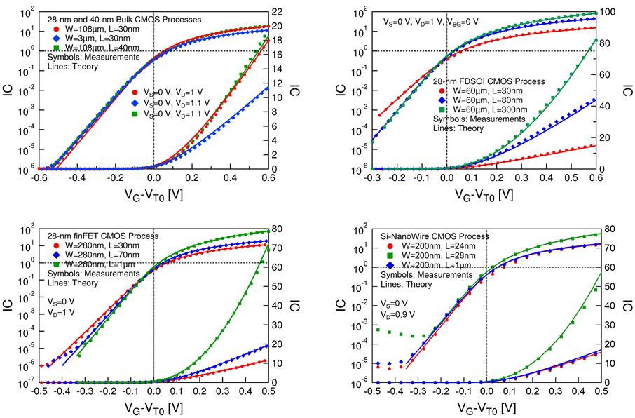
The objective of this project is to provide the designers a reliable instrument for an effective early-stage phase of the design, where all the trade-offs need to be identified and efficiently addressed. The concept of inversion coefficient replaces the overdrive voltage as the main design parameter covering the whole range of operating points from weak to strong inversion across moderate inversion. The simplified EKV-based model, despite the very few number of parameters, can successfully model the large- and small-signal behavior over a wide range of bias. It can be used for FDSOI, finFET and Si-nanowire processes, demonstrating also to act as a benchmark for different technologies.
Examples
The simplified EKV model has been validated with several CMOS processes, i.e. Bulk, FDSOI, finFET, Si-NanoWire. Despite its simplicity and the limited set of parameters, it demonstrates to be accurate. As an example, ID-VG curves from different processes and geometries are reported.