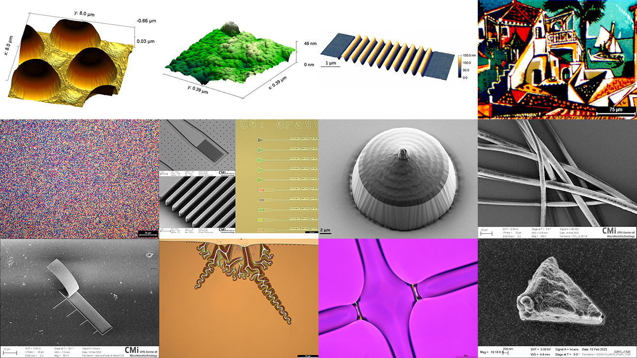
2026, January

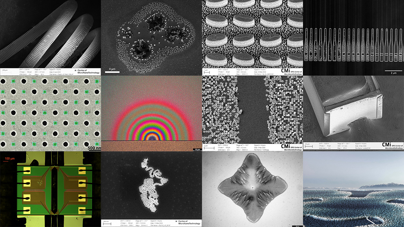
Choose your moon
Melania Coronese, NEMS
Alessio Zicoschi, LPQM
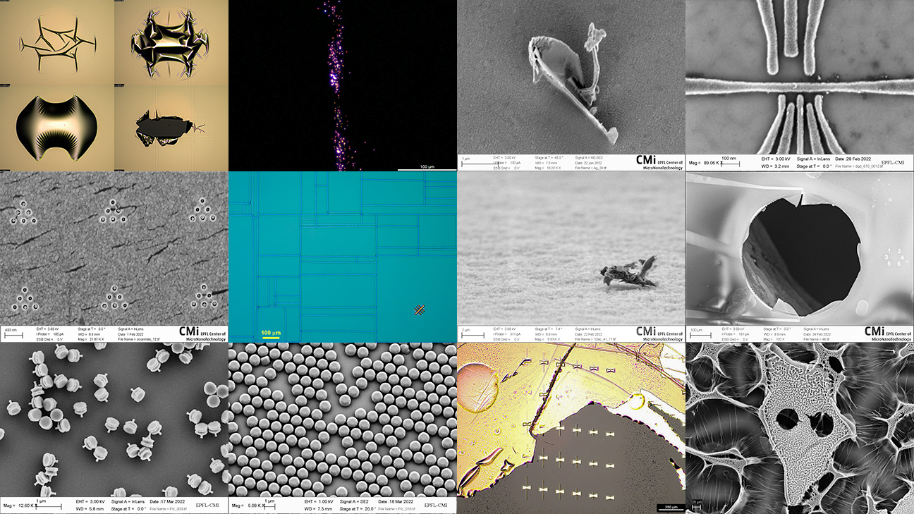
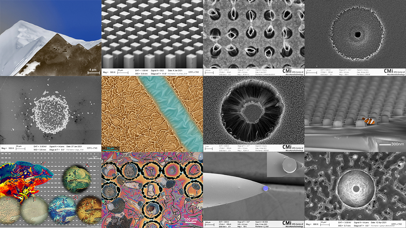
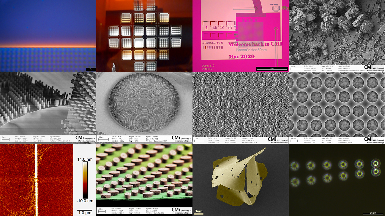
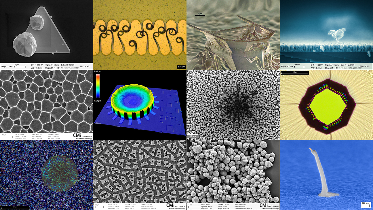
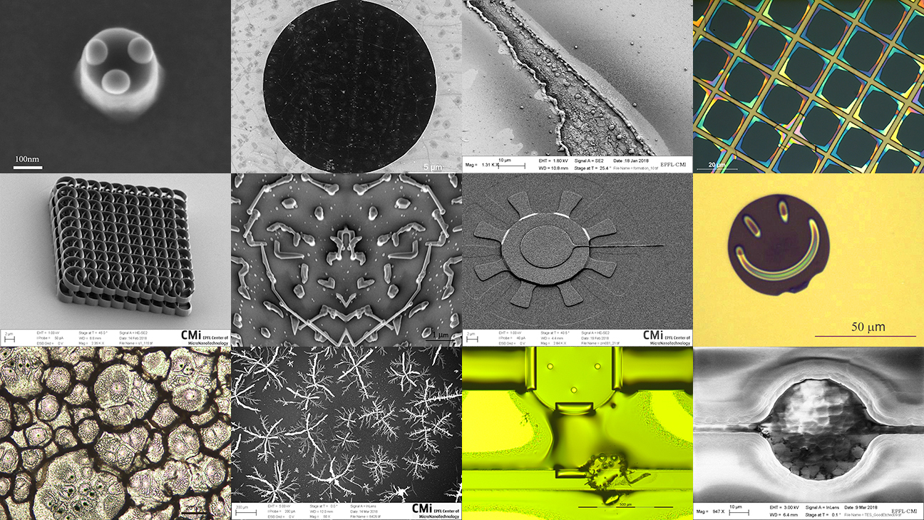
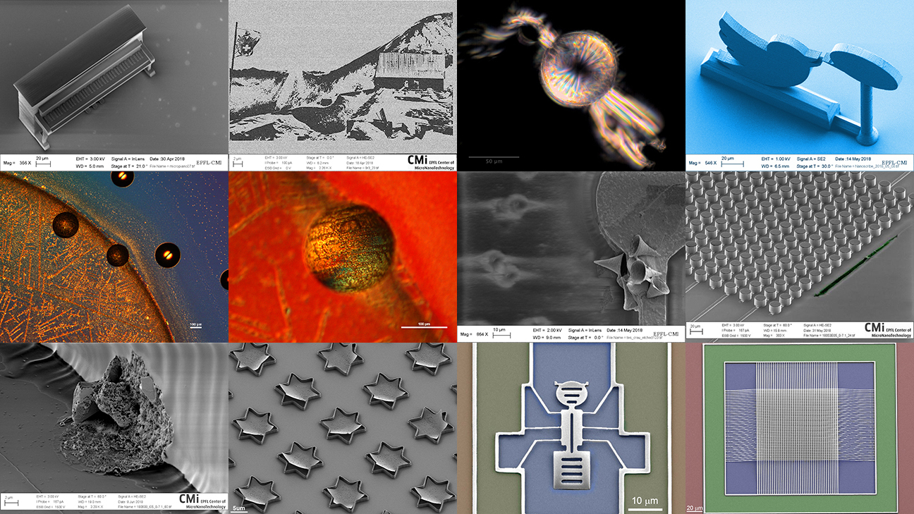
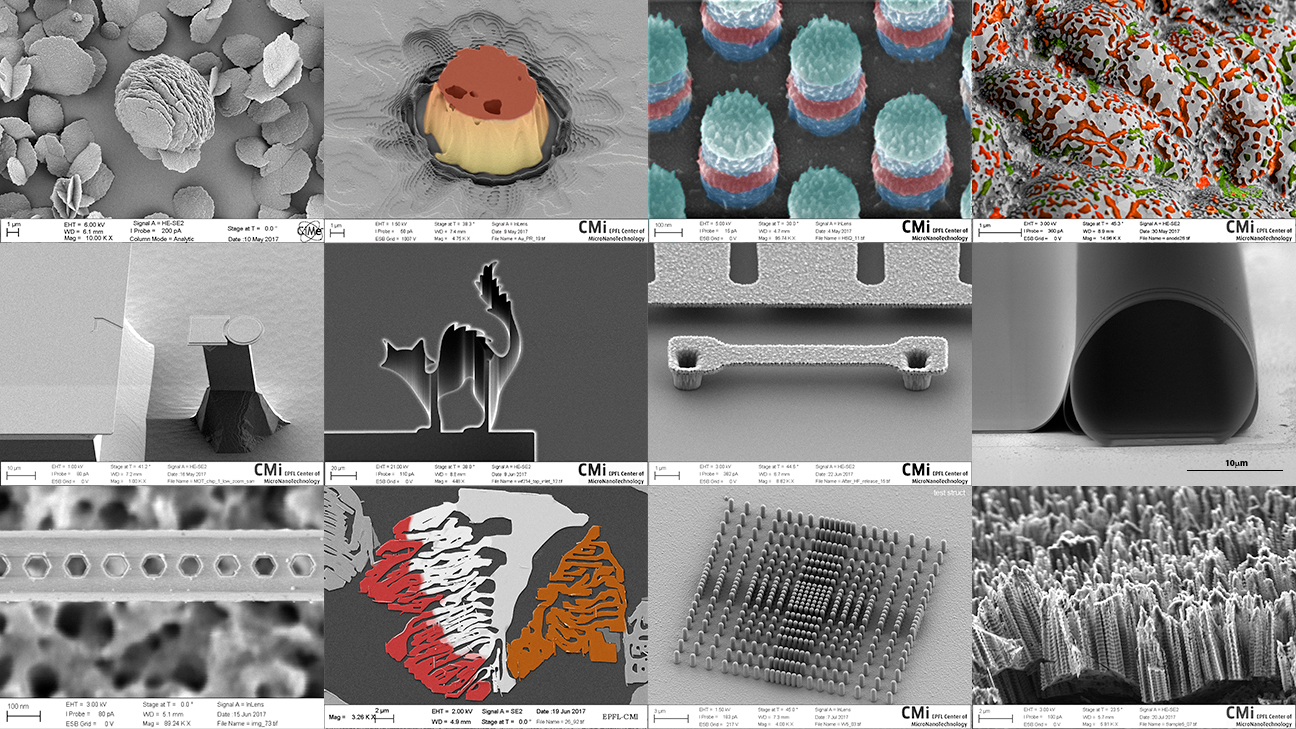
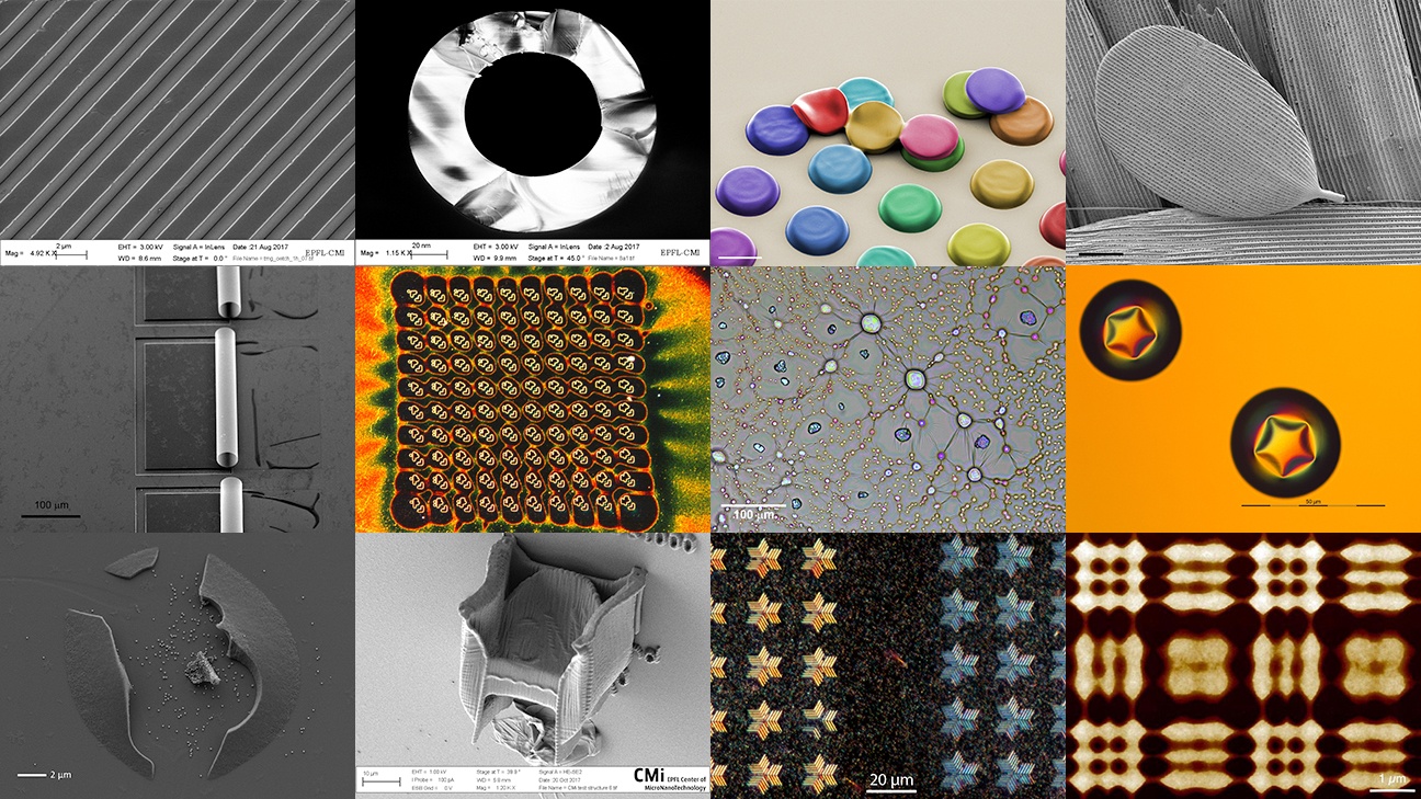
A constellation of moons born from tiny nanoholes, emerging from the darkness like impossible worlds, silently aligned in an artificial sky. An image captured through a dark-field microscope, where light reveals only what dares to scatter it.

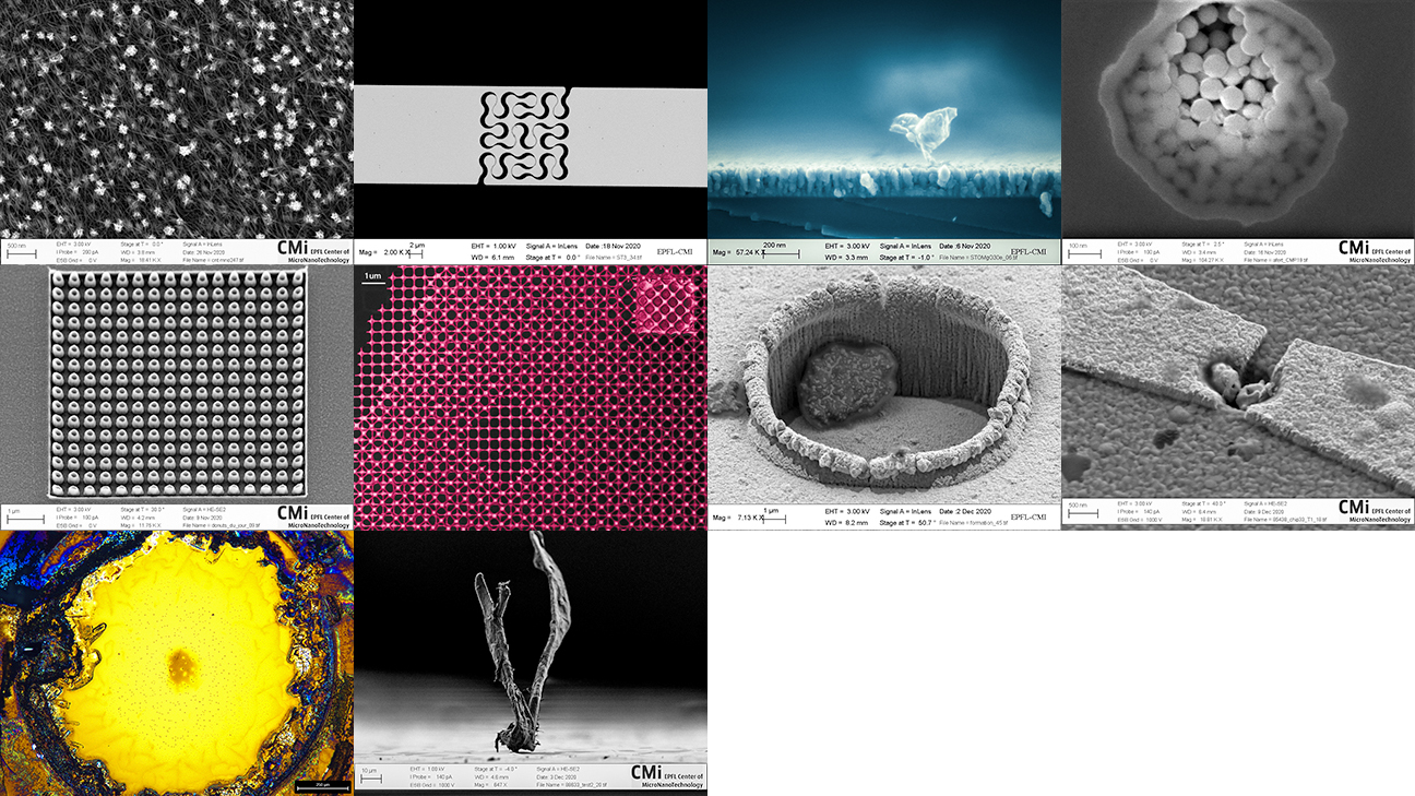
Rainbow ripple
Michael Smith, Sy&Se SA
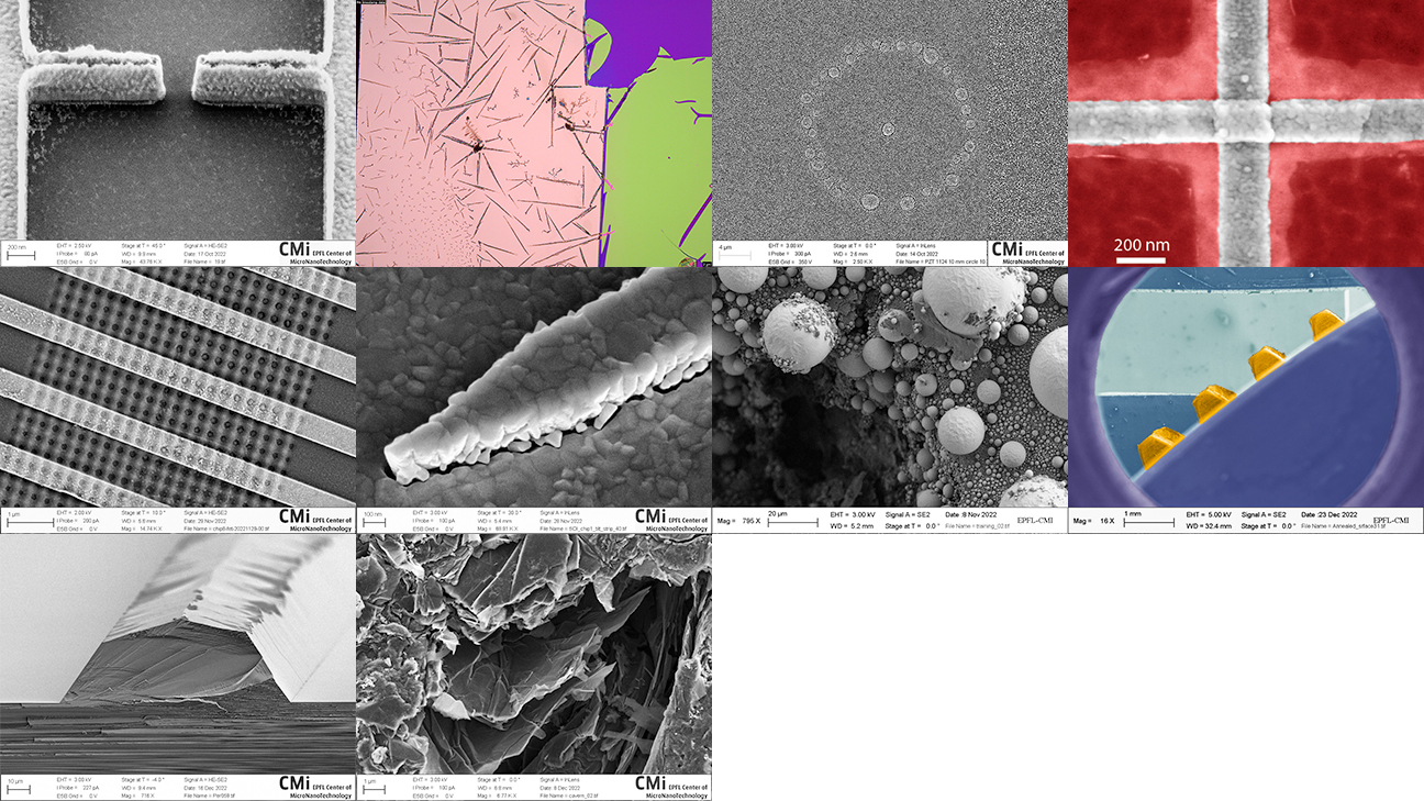
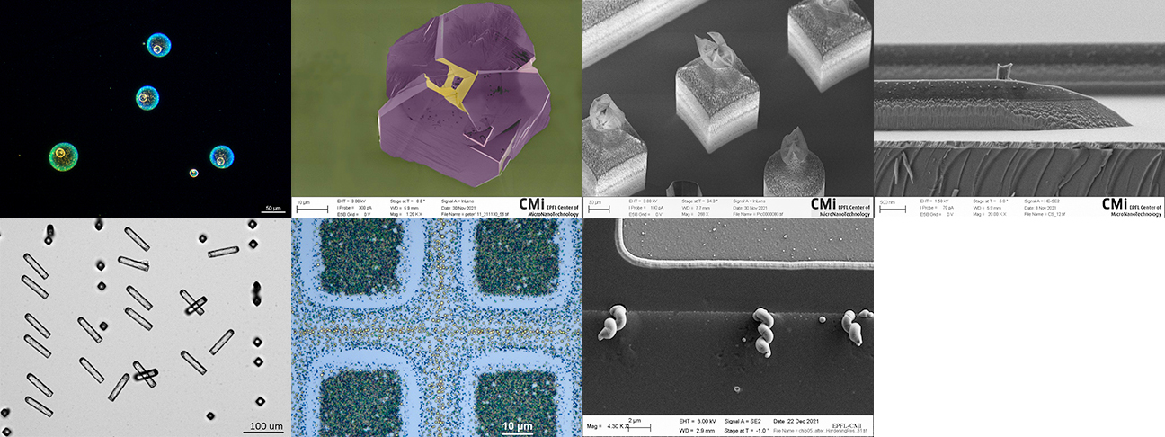
A void between bonded wafers of silicon and fused silica generates a colourful interference pattern of Newton’s rings. An etched cavity in the silicon wafer distorts the pattern, creating ripples in the interference fringes. The wafer cavities were fabricated using dry etching tools at CMi. The image was captured using a Leica optical microscope at CMi. The wafer bonding was performed with Sy&Se equipment.
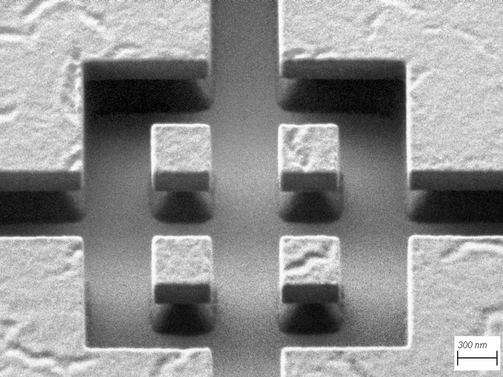
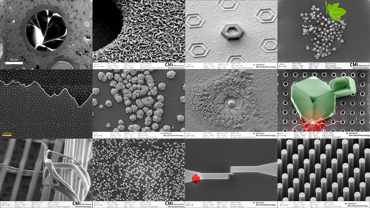
The Play of Shadows
Mohammad Rezaei, POWERLAB
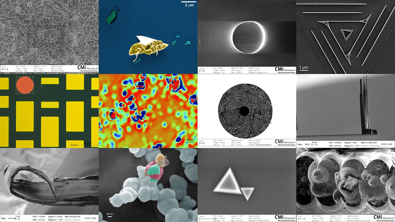
This SEM image captures a precisely sculpted nanoscale structure in a patterned resist stack, where sharp edges and suspended features cast dramatic shadows under low-voltage electron illumination. At a few hundred nanometers wide, the image turns an ephemeral fabrication step into an eternal landscape.
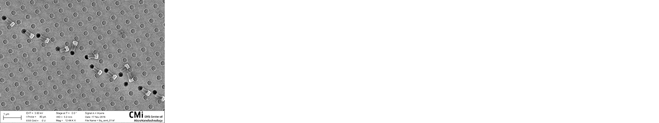
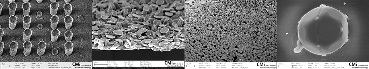
A Nanoscale Battlefield
Elif Nur Dayi, LNET
A snapshot of a serious battlefield at 50.000x. Warning: excessive doses during electron-beam lithography (EBL) may cause your amorphous Si nanopillars to develop combat skills.

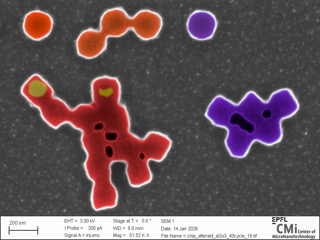
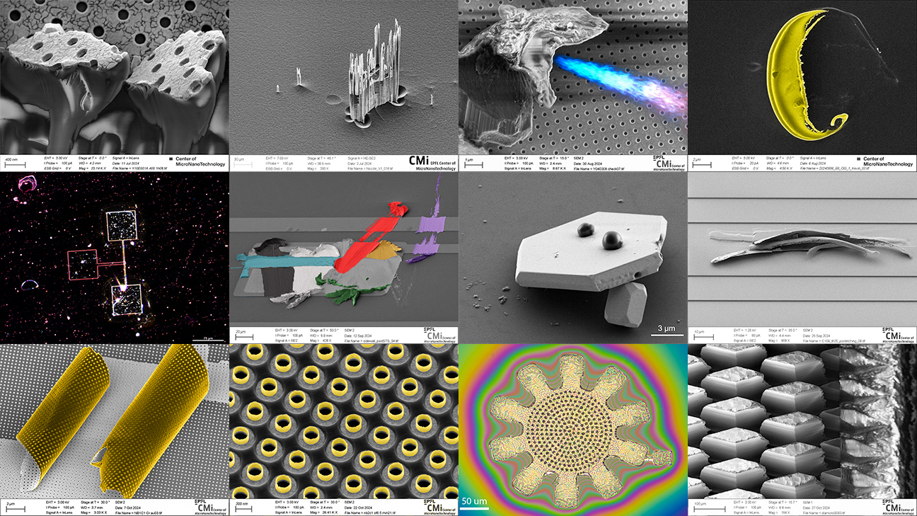
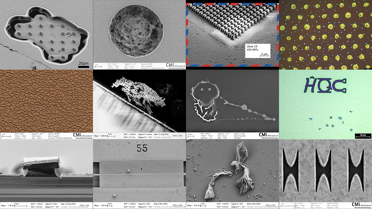
Gold rush on an aluminum layer
Mikhail Masharin, BIOS
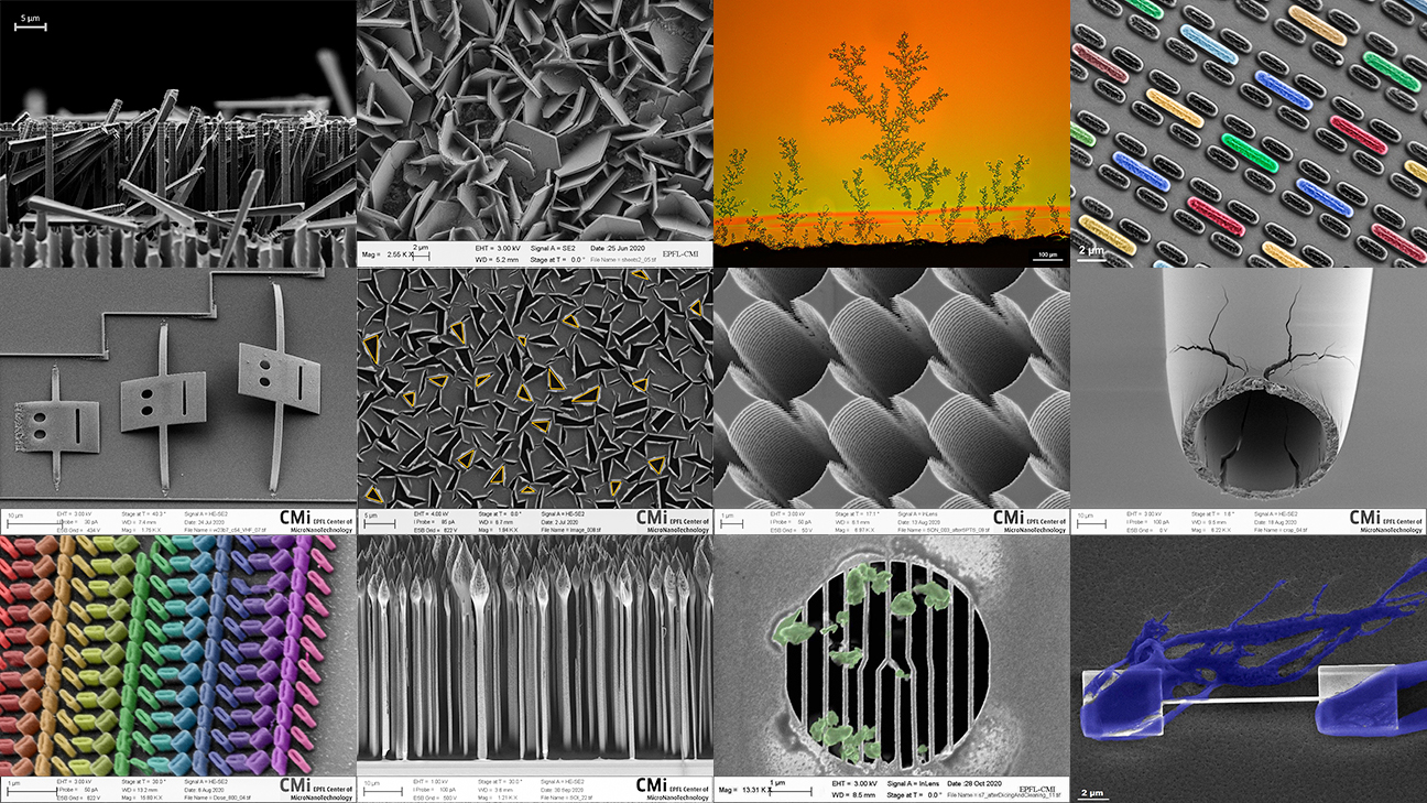
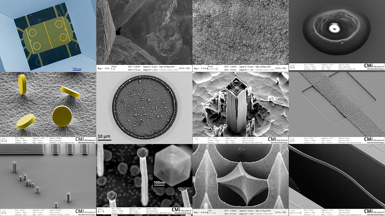
There is a hexagonal lattice of interconnected gold cylinders on top of the aluminum layer. The lattice geometry determines the optical resonances used for the various applications, such as optical sensing.
2025


2024
2023
2022
2021
2020
2019
2018
2017
2016