Available Projects for Students

Student projects in LMIS1
We offer a variety of projects for students for both semester and master projects in the field of Micro- & Nanoengineering. Mostly, the proposed projects are linked to our ongoing research topics for PhD projects, postdocs or senior scientist, that are funded by EPFL or third party funds (SNF, CTI/KTI, EU, etc). In that way, the student is involved in real-life topics with clearly assigned tasks that are complementary but in collaboration with the laboratory’s research staff. Alternatively, we also invite Master students to propose their own idea on the realization of a new technology or device in the field of Micro- & Nanoengineering. If you have a concrete idea, please don’t hesitate to talk to Prof. J. Brugger and Dr. G. Boero directly or to one of the staff members to see if a Semester or Master project can be defined around the idea generated by you.
Download all the available projects here
All student projects are also listed on IS-academia


Grayscale nanolithography for 2D nanoelectronics

While nanolithography has historically focused on downscaling, there is now a growing interest in grayscale nanolithography for introducing or enhancing functionality in micro-nanodevices applied to optics and fluidics. Grayscale thermal scanning probe lithography (t-SPL) achieves single-digit nanometer spatial resolution and sub-nanometer depth control. In t-SPL, a heated nanotip is used to pattern a temperature-sensitive resist. The fine control over the indentation depth of the tip via an electrostatic potential between the tip and the substrate allows the fabrication of grayscale patterns with high precision.

Grayscale topography engineering for 2D nanoelectronics

Type : Semester project / Master project

Section : Microengineering, Electrical Engineering, Materials Science

While nanolithography has historically focused on downscaling, there is now a growing interest in grayscale nanolithography for introducing or enhancing functionality in micro-nanodevices applied for optics and fluidics. Grayscale thermal scanning probe lithography (t-SPL) achieves single-digit nanometer spatial resolution and sub-nanometer depth control, but it has limited scalability. We combine t-SPL with nanoimprint lithography to replicate high-resolution grayscale nanostructures on large surfaces by step-and-repeat process [1, 2]. For the next generation of nanoelectronics, we use these deterministic grayscale topographies for strain engineering of 2D materials as they hold the potential to replace silicon in transistors with sub-10 nm channel lengths.

Figure 1: a AFM images and amplitude comparison of a sinusoidal pattern before (Line 1) and after (Line 2) dry etch transfer. b Fourier transforms of the measured topographies after t-SPL on PPA and transferred into SiO2. c Fabrication process flow of grayscale dielectric nanostructures for 2D materials strain.

The main tasks in the project will be:

  • Grayscale stamp fabrication by combining t-SPL and dry etching
  • Nanoimprint lithography and metrology characterization
  • 2D material strain characterization

Desired Skills:

  • Autonomy
  • Knowledge in cleanroom processes is a plus


References:

[1] Howell, Samuel Tobias, et al. “Thermal scanning probe lithography—A review.” Microsystems & nanoengineering 6.1 (2020): 1-24.

[2] Erbas, Berke, et al. ” Combining thermal scanning probe lithography and dry etching for grayscale nanopattern amplification.” ChemRxiv (2023)


Contact: Berke Erbas ([email protected])

Download PDF


Nanostencil for Single Ion Doping

At LMIS1 we are also taking part on the research for new quantum technologies by using nanostencils (consisting into a very thin Si3N4 membrane with nanoapertures patterned into it) as masks for the precise placement of single ions into silicon in order to use their nuclear or electronic spins as quantum entities to be utilized as qubits for quantum computing. We are currently exploring different strategies such as ion implantation or ion diffusion to achieve single ion doping and improve the state-of-the-art.

Chemical surface modification via stencil lithography

Type : Semester/Master project

Section : Microengineering, Physics, Materials Science

Stencil lithography is a high-resolution patterning technique based on the shadow mask principle which has been used since the ancient ages. In the last decades, this technique has evolved for the patterning of micro and nanostructures mainly for thin-film deposition, but also for etching and ion implantation. Using stencil for micro and nanopatterning offers some advantages compared to conventional lithographic techniques such as being an easily repositionable and reusable mask and the fact that allows to by-pass many steps of conventional lithographic techniques. Considering all these advantages, stencil may be a good candidate to explore to be used as a mask for the selective chemical modification of surfaces

The main objective of this project is to use stencils as masks for the selective chemical modification of the surface of a substrate so that then molecules binding specifically only to the chemically modified regions can be placed in the predefined pattern.

The initial idea is to study the effect of using stencils on an HF-pretreated silicon surface for an oxygen plasma treatment, but the student is welcome to bring new ideas for different chemical surface modification strategies.

Figure 1. Main idea and scheme of the process: (1)Si surface treated with HF, (2) Stencil is placed over the surface to be modified, (3) Oxygen plasma is performed to chemically modify the surface, (4) Stencil is removed

Work description:

  • Review state of the art of selective chemical surface modification and characterization.
  • Design and fabrication of micro and /or nanostencils at CMi cleanroom
  • Application of chemical modification strategies such as oxygen plasma using the stencil as a mask.
  • Characterization of the chemically modified surface.

Contact: Pol Torres Vila ([email protected])

Download PDF


The ROSE project

If you have no olfactory impairment, perhaps you are unaware of the importance of your sense of smell. Odors are sources of both pleasure and social bonding, they contribute to our emotional wellbeing, with reduced or absent olfaction being linked to depression. Loss of smell also increases the risk of household accidents (detection of noxious gases and smoke). It is estimated that partial or total loss of smell arising from a variety of causes (trauma, congenital deficits, age, viral infection and other pathologies) concerns about 20% of the population. Restoring olfaction – completely or even partially – is important for society, but a difficult challenge for science: a technological device capable of restoring odorant detection and recognition is currently being developed at LMIS1.

Microfluidic devices to study microalgae metal pollution

Type : Master/Semester Project

Section : Microengineering – Physics – Electric Engineering – Life Science

Pollution of terrestrial and aquatic ecosystems by heavy metals is a major and ever-growing threat to environmental and human health. A better understanding of the effects of toxic elements on land plants and microalgae is critical to develop approaches for treating contaminated environments using phytoremediation processes1.

The main objective of this project is to study the tolerance and accumulation of metals in a metal-hypertolerant green microalga of the Coelastrella genus. To do so, we plan to develop microfluidic devices2 for high-throughput screening of metal tolerance in this microalga. Your task will be to fabricate and characterize PDMS chips for single alga trapping that will later be used in fluorescence microscopic studies. You will work on a multidisciplinary project and start from literature and design, going to fabrication in the clean-room, experimental testing, and finally analysis. You will learn cell culture techniques, microfabrication, critical thinking and experimental know-how.

Prerequisites:

  • Interest for biological applications and microtechnology with background in one of them. Prior training in nano/micro- fabrication is an advantage
  • Independent and willing to have fun in the lab
  • Master projects will be preferred

References:

[1] Muthusaravanan, S. et al. Phytoremediation of heavy metals: mechanisms, methods and enhancements. Environmental Chemistry Letters 16, 1339–1359 (2018).

[2] Kim, H. S., Weiss, T. L., Thapa, H. R., Devarenne, T. P. & Han, A. A microfluidic photobioreactor array

Contact: Clémentine Lipp ([email protected])

Download PDF


Development of an olfactory prosthesis for people suffering from anosmia

Type: Master/Semester project or lab immersion

Section: Microengineering – Physics – Electric Engineering – Life Science

Sensory deficits are a major source of handicap in people’s lives. Scientists have already developed prostheses and implants for hearing impairments and are developing those for vision. Partial and total loss of smell (hyposmia / anosmia) impacts 20% of the world-wide population with deleterious effects on quality of life. However, we have yet to develop such devices to restore the sense of smell, primarily because scientific knowledge linking artificial systems to human biological olfaction is still lacking. The ROSE project is composed of a European consortium working together to push the limit of artificial olfactory sensations. The project will be held in close collaboration with the European partners and may include travels to meet with them.

At the LMIS1, we are currently investigating the new possibility of stimulating sensations in the nasal cavity using drugs known for their triggering of acute sensations. Thermal and piezo inkjet printing methods have been identified as promising tools to achieve that goal thanks to their easy actuation mechanism, control in droplet formation mechanism and integrability.

The project thus comprises the definition of the requirements of such a device to be compatible with medical devices regulations to ensure the patient’s safety. Also, the possibility of using components existing on the market will be evaluated. The project will redirect to microfabrication technologies in the case where this option was not possible. The topic is highly multidisciplinary, involving aspects of physiology electronics, cleanroom microfabrication and materials science: the focus can be adjusted depending on the student’s preferential interests, best knowledge, previous experience and motivation.

Figure 1 : (a) schematic showing the olfactory system (b) Paradigm of the ROSE project for the restauration of olfaction in anosmic people

Possible tasks:

  • Analysis of droplet formation mechanism and assessment of different methods
  • Electronics design for the control of droplet formation
  • Experiments for the characterization of droplets formation
  • Design, optimize and/or execute process flows at EPFL’s state-of-the-art CMi cleanroom:
    • Process flow conception,
    • Drawing individual devices and aggregated chip/wafer lithography layouts,
    • Characterization of the resulting components using SEM, AFM, and other metrology tools.

Contact: Clémentine Lipp (clementin.lipp @epfl.ch)

Arnaud Bertsch ([email protected])

Download PDF


Additive Manufacturing for Therapeutic Delivery Devices

In LMIS1 we are currently developing therapeutic delivery devices that encapsulate various therapeutic cargos using additive manufacturing technology. The high degree of freedom in design and materials in additive manufacturing technology (AM) enables device adaptation for personalized therapeutic. Further incorporation of biodegradable materials and active release methods into our device will expand the technique’s applicability.

Fabrication of lipid microstructure for oral drug delivery device

Type : Master/Semester project

Section : Microengineering, Mechanical Engineering, Bio engineering, Materials Science

Co-administration of poorly water-soluble drugs with lipid formulations can enhance the bioavailability of these drugs. Administration of drugs encapsulated lipid formulations can be the one way of achieving this. Recently fabricating the various design of drug-lipid formulations enabled by the development of additive manufacturing techniques. However, most of the device’s dimension is limited to mm to cm. Thus, limiting the versatility of the device’s pharmacokinetics. Melt electro writing is an attractive tool for decreasing the device’s resolution to the micrometer size. The goal of this project is to fabricate lipid drug delivery devices using melt electro writing. Throughout this project, you will prepare and optimize the melt electro writing condition of lipid drug formulation. Then you will investigate the effect of the design, dimension, drug types, lipid types on the device’s drug release. Hence the first half of the project will focus on preparing various lipid-drug formations and optimizing their printing condition. And the last half will be focused on printing devices with different designs, and measuring and analyzing their drug release profile.

Figure 1. From right to left:  Melt electro writing tool setup, Lipid Taylor corn, Lipid chess board structure                                                    

Work description :

  • Preparation of lipid-drug formulation
  • Optimizing the melt electro writing condition of lipid-drug formulation
  • Fabricating various designs, dimensions of the lipid-drug device
  • Measuring and analyzing the drug release profile of the device in digestive system mimicking environment.

Contact : Jongeon Park ([email protected])

Download PDF


Acoustically mediated drug delivery device with frequency selectivity

Type : Master/Semester project

Section : Microengineering, Mechanical Engineering

Actively controlled release function is important for implantable drug delivery device. Because we can achieve sophisticated and personalized treatment according to the patient’s feedback after the implantation. Acoustic field is suitable for external stimulus for active controlled release due to its body penetration ability, biocompatibility, and low manipulation power. When acoustic field exposed to the drug solution encapsulated device, acoustic pressure cause by standing waves give stress to the sealing layer. Acoustic harmonic frequency of the device which gives maximum vibration can be tuned by changing the design of the capsule. By using this phenomenon, we can selectively open the sealing layer of the device with different shape. (Figure 1) This project will mainly compose of the two-part simulation and design part and test part. For the simulation and design part, you will design and optimize the device structure according to the simulation results of its vibration force distribution to device in a fluid environment under acoustic wave exposure. For the test part, you will set up the platform for acoustically mediated drug release experiment. The simulation will be 6-7 weeks and fabrication of the prototype and acoustic release test will take 7 weeks.

Figure 1. Right to left:  Concept of the project, Initial simulation results: Stress applied on sealing layer according to the frequency.

Work description:

  • COMSOL simulation to figure out each design’s harmonic frequency which give maximum stress to the sealing layer
  • Setting up the platform for acoustically mediated drug release experiment.
  • Acoustically mediated drug release experiment

 Contact : Jongeon Park ([email protected])

Download PDF


Additive Manufacturing for Biomedical Applications

At LMIS1, we are expanding our capabilities in micro manufacturing of biomaterials using 3D printing. Melt electrowriting (MEW) is an electrohydrodynamic 3D printing technique which involves processing of polymer melts into micron sized fibers (5-100 microns) using high voltage as the driving force. The fibers can be deposited in a layer-by-layer manner to make 3D printed constructs. The 3D printing can be done in desired patterns to produce a wide range of mechanical properties.

3D printing (fused deposition modelling) of metallic tubes with complex geometries

Type : Master/Semester Project

Section : Microengineering, Bio Engineering, Materials Science, Robotics

Fused deposition modelling (FDM) or fused filament fabrication is a 3D printing technique where a polymer melt is extruded through a nozzle onto a temperature-controlled build platform. A three-dimensional structure is successfully created by stacking the extruded polymer layer-by-layer. For most applications and structures, a flat build plate is usually sufficient. However, it can be limiting in some cases where fine features are required as overhangs and some post processing techniques like sintering are to be employed on the printed object.

Figure 1. Schematic representing the idea of tubular collector on FDM printer (left). Potential design ideas for printing (right) 2mm scale. Diamond or auxetic designs to be tested using metal filled filaments.

A FDM printer usually uses a standard polymer filament with 1.75/2.85 mm diameter. A large variety of polymers have been processed using this technique with poly lactic acid (PLA) being the most utilized due to the ease in processability. Other materials such as Nylon, flexible thermoplastic urethane and fiber reinforced polymers have also been used and are available commercially. There is increasing interest in composite materials, specifically metal filled and ceramic filled polymers which can be used in FDM. The printed parts from these materials can be sintered (high temperature treatment) to obtain fully metallic and ceramic components.

This student project will involve building of a new Voron FDM printer and upgrading it for temperature controlled tubular collector. Once the software control is stablished for printing complex tubular structures, the idea will be to implement real-time monitoring of printing through image analysis. The next part of the project will involve printing of metal/ceramic filled polymer filaments with minimum resolution feasible. The printed parts will be sintered and analyzed to further optimize the FDM approach to obtain fully metallic/ceramic tubular constructs.

Possible tasks:

  • Incorporating tubular collector on Voron 0.
  • Temperature control of the collector.
  • Software control for printing complex geometries with minimum resolution.
  • Testing composite materials to print functional constructs (metal or ceramic filled FDM filaments).

Useful reading: Hong et al, Open5x: Accessible 5-axis 3D printing and conformal slicing (https://dl.acm.org/doi/10.1145/3491101.3519782)

Contact: Biranche Tandon ([email protected])

Download PDF


3D printing (Melt electrowriting) with bioderived polymer for drug coated wound dressings

Type : Master/Semester Project

Section : Microengineering, Bio Engineering, Materials Science, Robotics

Melt electrowriting is a quickly advancing additive manufacturing technique which utilizes a large electrical voltage to stretch a polymer melt extruded through the nozzle into fibers down to micron range and precisely deposit them into desired patterns. The obtained product is often termed as a scaffold in literature. These scaffolds are flexible, light and easy to handle. The properties of the produced structures are tailorable by altering the deposition pattern, fiber diameter and the material used for printing.

Figure 1. Overview of the principle and parameters involved in MEW (left). Scaffold designs which will be potentially explored (right).

A large variety of polymers have been processed using this technique with poly caprolactone (PCL) being the most utilized due to ease in processability and very limited degradation of the polymer at its melting temperature. PCL has been processed into a large variety of designs or patterns (Figure 1A). Depending on the chosen design, the scaffolds have different mechanical properties and induce a different biological response.

At LMIS1, we have MEW printers which are capable of printing polymers with a melting temperature range from 30-250 °C. Our current projects involve printing of PCL and shape memory polymers. The goal is to expand MEW processability to bioderived materials.

This student project will contribute towards establishing 3D printing protocol using commercially available bioderived polymer filaments (poly hydroxy alkanoates (PHA)). PHA is a bioderived polymer which degrades without the release of microplastics in the environment. The aim will be to process PHA based polymer for MEW and fabricate various micro-fiber structures with tunable mechanical properties

Possible tasks:

  • Characterization of filament and printed materials using FTIR, DSC, SEM, etc.
  • Parametric optimization of melt electrowriting.
  • Coating of printed materials with drug/polymer composite.
  • Study the drug release behavior.

References:

1]  Robinson et al (2019) Advanced Functional Materials, volume 29, Issue 44.

[2]  Hochleitner et al (2016) BioNanoMaterials, volume 17, Issue 3-4.

Contact: Biranche Tandon ([email protected])

Download PDF


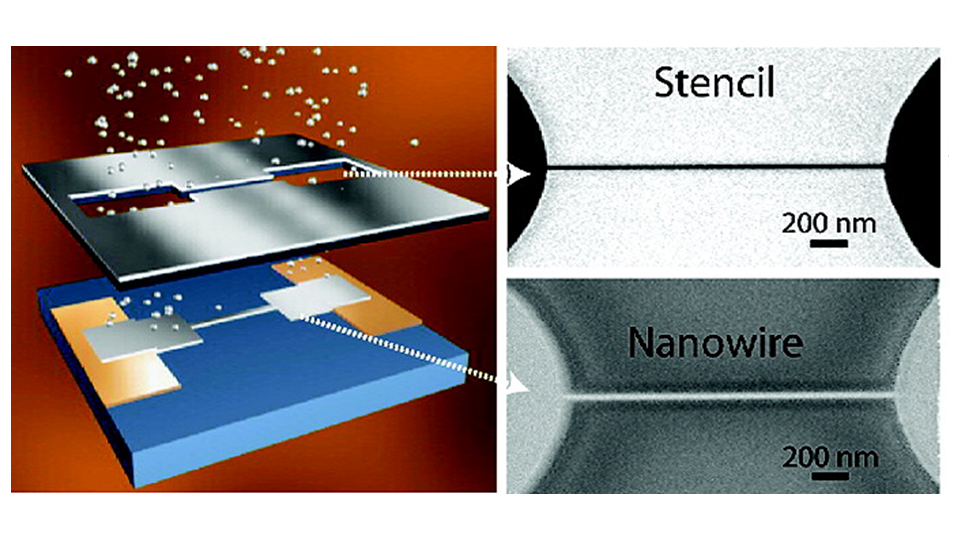
Transient electronics made by stencil lithography

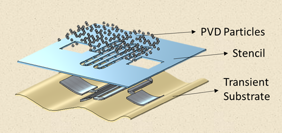
At LMIS1, our research efforts in stencil lithography have yielded significant advancements. The recent invention of the bridge stencil has allowed us to pattern a wider range of shapes with greater precision. Expanding on this success, we are now shifting our focus to materials. Leveraging the resistless nature of stencil lithography and its ability to avoid liquid processes, we aim to utilize transient materials like magnesium and zinc for patterning. Our ultimate objective is to establish an electronic library in transient form, showcasing the potential of stencil lithography in the patterning of more kinds of materials.

Designing and Validating Bridges on Stencils: Calculation, Simulation, and Verification

Type: Master/Semester Project

Section: Microengineering – Physics – Materials Science

Stencil lithography is a resistless micro-fabrication method using a silicon nitride film stencil for pattern deposition or etching.[1] It enables sub-nanometer scale patterns without the need for photoresist or liquid environments. However, challenges include the inability to pattern closed-loop designs due to film detachment, and the risk of stencil curvature or breakage caused by inner stress. Researchers have explored stencil movement during deposition and other approaches to address these issues.

At LMIS1, a new solution was proposed, incorporating auxiliary bridges in stencils. These bridges serve dual purposes: securing the suspended part of the stencil and preventing membrane curvature. By maintaining a specific gap between stencil and substrate, blurring effects during deposition ensure continuous pattern coverage beneath the bridges. Extensive measurements of morphology and electrical properties have validated the effectiveness of the bridge stencil.

The focus of this student project will be on optimizing the design parameters of the bridge stencil. This includes investigating the width and density of bridges, determining their optimal placement, and establishing the ideal gap between the stencil and substrate. The ultimate goal of the project is to develop a set of guidelines for the automated design tool for bridge stencils.

Figure 1 : The concept of bridge stencils and the blurring effect. a,b) Schematic drawings showing the use of bridges for a) realizing unfeasible geometries on stencils (e.g., close-loop circular apertures), and b) suppressing the bending of cantilevers for meandering apertures. c,d) Schematic drawing showing the beneficial use of the blurring effect. [2]

Possible tasks:

  • Conduct stress calculations in simple models to analyze the relationship between bridge parameters and stress levels.
  • Simulate stress distribution in complex patterns (e.g., circles, serpentines) to guide optimal bridge placement.
  • Verify the concept of bridge placement in the clean room.

References:

[1] O. Vazquez-Mena et al, vol. 132, pp. 236–254, Jan. 2015.

[2] Y.-C. Sun et al, Adv. Mater. Technol., vol. n/a, no. n/a, p. 2201119.

Contact: Chenxiang Zhang ([email protected])

Download PDF


Mixed reality learning for microfabrication practical

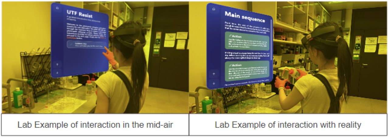
At LMIS1, we are currently embarking on a novel journey to integrate mixed reality into learning methods for microfabrication processes. This approach presents a promising avenue as it allows hands-free interaction and diminishes cognitive load during learning. Our research is dedicated to creating interactive mixed-reality content to revolutionize microfabrication and cleanroom training practices. As we scrutinize the effectiveness and feasibility of multimodal learning within a mixed reality framework, we are embracing various learning strategies including gamification, scaffolding, and multimodal interaction.

Development of interactive microfabrication course through Mixed Reality (MR)

Type: Master/Semester Project

Section: Microengineering – Electric Engineering – Computer science (IC) – Human-computer-interaction

One of the most promising advancements in students learning benefit is mixed reality (MR) technology[1,2]. MR has the potential to revolutionize education by offering new ways of teaching complex concepts and fostering deeper understanding with multimodal information while reducing the cognitive load.This is particularly relevant in technical fields like microfabrication, where traditional learning methods may not fully capture the intricacies of the subject matter, and the practical course requires hands-on experiment so that students could succeed in building complete fabrication processes. As MR technology continues to gain traction in educational settings, it is crucial to investigate its effectiveness and determine the optimal integration of MR with traditional learning approaches.

At the LMIS1, we are currently investigating new possibilities of providing an interactive MR learning material for the microfabrication process, cleanroom training, etc. By investing the difference of multimodal learning with mixed reality, we have combined different 3D model, figures, videos, anchors, texts, etc into the existing HoloLens 2 Mixed reality goggles.

This student project will contribute to enhance the interactables of the system, either by add interactive functions such as gamification or by hand interactions, The topic is highly multidisciplinary, involving aspects of human-computer interaction, understanding or interest of microengineering, and cleanroom microfabrication. The focus can be adjusted depending on the student’s preferential interests, best knowledge, previous experience and motivation.

Figure1: Combination of virtualism and reality in HoloLens for the microfluidics lab. De Micheli, A. J., Valentin, T., Grillo, F., Kapur, M., & Schuerle, S. (2022). Mixed Reality for an Enhanced Laboratory Course on Microfluidics. Journal of Chemical Education, 99(3), 1272-1279.

Figure2: HoloLens 2, https://learn.microsoft.com/en-us/hololens/hololens2-industrial-edition-faq

The main tasks in the project will be:

  • Conduct research, design, programming phrases of product (adjustable);
  • Interaction development based on brand new Microsoft Mixed Reality HoloLens 2
  • Cooperate with the course designer to integrate the content and optimize it.

Desired Skills:

  • The Hololens development is based on C# Programming in Unity 3D, it’s better if you have experience on that, if not, we prefer you are fluent at java or C++ or Python, at least one programming language;
  • Knowledge in TCP\IP communication, server maintenance is a plus
  • Knowledge in cleanroom processes is a plus

What you will gain:

  • Experience of conducting research, designing, engineering phrases of product;
  • Collaboration, communication, and nice group friendship.

References:

[1]  Fisch, S. M. (2017). Chapter 11 – Bridging Theory and Practice: Applying Cognitive and Educational Theory to the Design of Educational Media. In F. C. Blumberg & P. J. Brooks (Eds.), Cognitive Development in Digital Contexts (pp. 217–234). Academic Press.

[2] Gattullo, M., Laviola, E., Boccaccio, A., Evangelista, A., Fiorentino, M., Manghisi, V. M., & Uva, A. E. (2022). Design of a Mixed Reality Application for STEM Distance Education Laboratories. Computers, 11(4), Article 4.

Contact: Qinglan Shan (qinglan.shan @epfl.ch)

Download PDF


Cryogenic Microwave Thermometry

At LMIS1 we are currently assessing possible alternatives to state-of-the-art 4-wires thermistors for cryogenic thermometry in ultra-low temperature systems (i.e. < 90 K). High quality factor superconducting resonators are investigated in order to explore the fundamental T-variations properties related to Cooper pairs kinetic inductance changes, with the final goal to sense cryogenic temperatures by means of resonance frequency shifts.

Superconducting Thin Film Microwave Resonators for Cryogenic Sensing

Type : Master/Semester project

Section : Microengineering, Physics, Electronic Engineering

Distributed physical measurements are essential in cryogenic systems in a variety of fields. Classical sensing approaches usually present a series of inconveniences, such as feedthrough space requirement, risk of leaks, risk of electric breakdown, heat input (conduction in wires), need for thermalization, etc… Allocating large number of sensors or compensating for the absence of distributed measurement imposes important constraints in the design of the cryogenic setup.

To overcome these drawbacks, we are currently investigating new possibilities of providing measurement systems in cryogenic environments (T < 90 K) by means of superconducting RF lumped elements resonators, which can be read in large numbers on a single RF line. Such a goal would be achieved either by exploiting variations of superconducting kinetic inductance [1-2], or by designing devices able to exhibit remarkable changes of geometrical LC parameters. Furthermore, the possibility of strategically nano-structuring the devices can allow to exploit more exotic superconducting phenomena to enhance sensing performance.

This student project will contribute to enhance such resonators, by investigating thin film nano-structuration methods on different materials. Subsequently, nano-engineered devices will then be fully tested and characterized in cryogenic environments (T < 90 K) using liquid He and cryostats.

Figure 1 : (a) schematic showing the superconducting resonator chip coupled to a standard Cu PCB; (b) optical microscope picture of a sensing device, showing the antisymmetric CPW B-field coupling of a thin film (e.g. NbTi) S-shaped Split Ring Resonator; (c) SEM picture of a test micropatterned YBCO film, courtesy of R. Russo.

The topic is highly multidisciplinary, involving aspects of condensed matter physics, RF electronics design and test, cleanroom microfabrication and materials science. At the end of the thesis the student will have gained a deep insight into sensing through superconducting phenomena, microfabrication in cleanrooms, and RF-cryo characterization.

Possible tasks:

  • Simulate, analyze and design superconducting RF components and resonators.
  • Design, optimization and execution of process flows at EPFL’s state-of-the-art CMi cleanroom:
    • Process flow conception.
    • Elaboration of microfabrication layouts.
    • Characterization of the resulting components using SEM, AFM, and other metrology tools.
  • Cryo-RF characterization of finalized devices in a cutting-edge experimental setup.

References:

[1]  P.K. Day et al. (2003) Nature 425 817.

[2]  H. Yu et al (2022) SN Applied Sciences 4:67.

Contact: André Chatel (andre.chatel @epfl.ch)

    Hernán Furci ([email protected])

Download PDF


ESR and NMR Spectroscopy

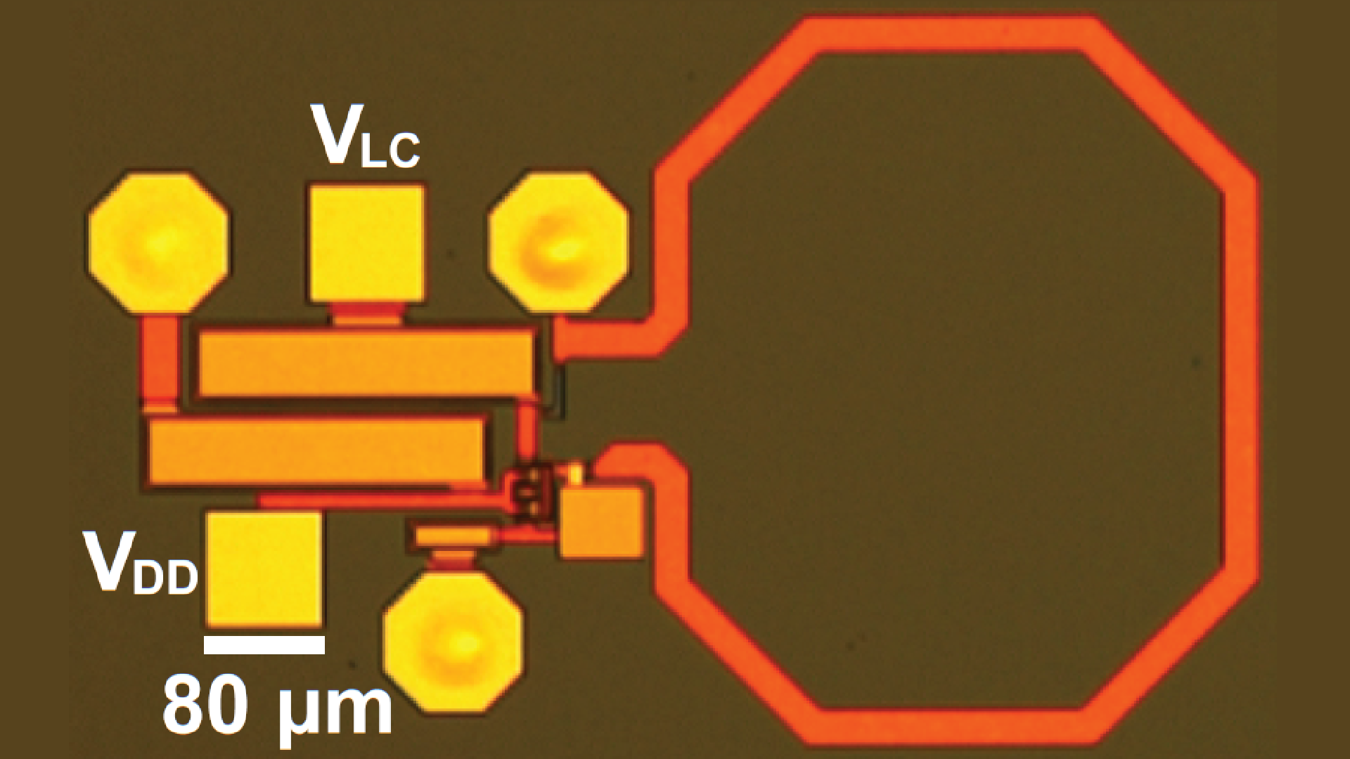
Electron Spin Resonance (ESR) spectroscopy is a widely used technique for the recognition of chemical radicals and species. At LMIS1 we are currently working on the optimization of ESR sensors’ sensitivity, especially for samples in the nanoliter and sub-nanoliter range, through the use of superconducting resonating structures.

Superconducting RF Resonators for Electron Spin Resonance

Type : Master/Semester project

Section : Microengineering, Physics, Electronic Engineering, Materials Science

Electron Spin Resonance (ESR) is a well-established characterization technique. In order to excite the spin ensembles a microwave signal needs to be provided. The sensitivity of this method is depending on many parameters. Among those parameters, one of the most important is the resonator quality factor, which, if increased, could boost the sensor’s sensitivity. Resonators realized with superconducting materials allow to achieve higher quality factors with respect to those made of ordinary metals. Many examples of those resonators already exist in literature, realized with materials such as Nb [1-2] and Al [3].

At LMIS1, provided the application related constrains, we are currently investigating different designs and different superconducting materials to realize superconducting resonators, mainly low temperature superconductors (LTS) such as NbTi and NbTiN.

This student project will focus on developing and optimizing a fabrication process for YBCO, a high temperature superconductor (HTS). The process flow will be used to fabricate high quality factor superconducting resonators by optimizing the fabrication parameters, with the main goal of realizing a material independent and high patterning accuracy microfabrication process. The resulting resonators will be characterized in cryogenic environments (T~77 K) using liquid N2. The topic is highly multidisciplinary, involving aspects of condensed matter physics, RF electronics design and test, cleanroom microfabrication and materials science: the focus can be adjusted depending on the student’s interests, best knowledge, previous experience and motivation.

Figure 1 : Thin film, superconducting coplanar waveguide resonators. Top Left: pattern example of a thin Nb film resonator [1]. Top Center: transmission frequency behavior of a Nb resonator [2]. Top Right: resonance frequency detail of an Al resonator [3]. Bottom Left: SEM image of first fabrication attempt on YBCO film.

Possible tasks:

  • Optimize superconducting RF resonators design to increase resonator quality factor.
  • Design, optimize and execute process flows at EPFL’s state-of-the-art CMi cleanroom:
    • Process flow conception
    • Drawing individual devices and aggregated chip/wafer lithography layouts,
    • Characterization of the resulting components using SEM, AFM, and other metrology tools.
    • Process flow optimization for pushing resolution and resonators’ quality factor.
  • Cryo-RF characterization of finalized devices in a cutting-edge experimental setup.

References:

[1]  Eichler et al. (2017) PRL 118, 037701;

[2]  Sigillito et al. (2017) Nature Nanotechnology 12, 958-962;

[3]  Bienfait et al. (2015) ) Nature Nanotechnology 11, 253-257.

Contact: Roberto Russo ([email protected])

Download PDF


Reconfigurable Photonic Integrated Circuits

Photonic equivalent of FPGA, Reconfigurable PICs can be implemented by using different physical mechanisms at nanoscale. We focus on the integration of Phase Change Materials on the standard silicon photonics platform to provide non-volatile components and on-chip photonic functions and systems.

Scalable Integration of Phase Change Materials onto the Silicon Photonics Platform

Reconfigurable Photonic Integrated Circuits (RPICs) are increasingly relevant in nowadays communications-dominated world, to route, (de)multiplex, process and convert light signals used as information carrier.

The sustainability of RPICs requires that these systems can change their configuration fast, that they be compact both in chip and overall system size, that they have low loss, and that in steady state they have a low power consumption. Phase change materials (PCMs) integrated onto standard silicon photonic platforms can be game changer in this matter, since they would enable complex but compact optical networks with non-volatile configurations, i.e. no energy is required in steady state to maintain the components in the desired state.

PCM are materials that have very distinct refractive index and absorption coefficients depending on whether they are in crystalline or amorphous phase. PCM with low optical loss have recently made their entrance in the field of integrated photonic components. However, nowadays no clear path has been identified for a scalable integration and nano-patterning of these materials on a standard photonic platform, with high production throughput techniques and integrated actuation.

In this project we seek to demonstrate the integration of PCM on SOI standard platform using DUV lithography at wafer-scale only, with integrated electrical actuation for the PCM transition. We will also design, fabricate and test novel photonic components based on this integration concept.

The student will contribute to:

– design and simulation of photonic components,

– implementation of lithography layouts,

– microfabrication runs in cutting-edge EPFL cleanrooms (where we can access an ASML DUV Stepper),

– mise-à-point of different steps of the overall process

– fabrication of SOI wafers / chips running full process.

– characterization of photonic chips.

At the end of the thesis it is expected to perform an assessment of the capabilities of the proposed photonic design and fabrication flow based on the performance of the finally obtained devices. Bringing to maturity this technology will revolutionise the field of programmable PICs. 

The student will work closely with the Principal Investigator Dr. Hernán Furci.

Full description

Contact: Hernan Furci ([email protected])