Our main activities are carried out in CMI (Center for Micro / Nanofabrication). Some specific research tools however are located outside cleanroom as listed below. They can also be used by other researchers. In case of interest, please contact the responsible scientist or Prof. Brugger directly.
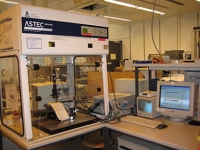
Automatic Inkjet Station
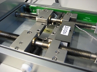
Inkjet printing has been recognized as an emerging technology and its first full-scale application has been in the display industry. Even though common photolithography is widely used in fabricating a variety of micro-devices and is a more advanced technology in terms of resolution, accuracy, versatility, scalability and reproducibility, it consists of many steps, leading to long process times. For ink-jet printing research, we have two ink-jet stations having fixed position of the ink-jet head with the computer controllable x-y-q stage, one is microfab and the other is microdrop. The configurations to generate drops from the nozzle between two machines are different. Moreover, specifications are as following.
|
Specifications:
|
|
Specifications:
|
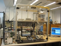
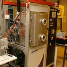
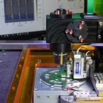
Full Wafer Scale Dynamic Stencil Lithography System
The full 100 mm wafer scale dynamic stencil lithography tool is developed based on UNIVEX 450B evaporation system. Quasidynamic (step-and-repeat) and dynamic (continuous stencil movement during deposition ) modes can be achieved during material deposition. Computer-controlled XY and Z positioning stages located inside an HV deposition chamber allow precise 3D movement of micro-machined low-stress silicon nitride membranes with respect to a static substrate.
  |
Specifications:
|
LINKAM Tensile Stress Tester (TST 350)
The system provides the ability to accurately characterize the tensile properties of your sample relative to temperature utilising the 0.001N sensitive force transducer and capture high resolution images of the structural changes.
 |
Specifications:
|
Submersible Transducers (Megahertz Sonicator)
The Megasonic system has a completely encapsulated transducers made of stainless steel, which is positioned at the bottom of an existing tank. The extremely uniform energy transmission ensures a hitherto-unachieved cleaning performance, while at the same time providing the best protection to the microstructures.
 |
Advances:
|
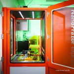
Nano Frazor (NF)
The Nanofrazor explore is a brand new tool aimed the fabrication of the nanoscale-structures. This technique facilitates thermal scanning probe nanolithography concept – direct write-patterning of the resist with the heated probe. Through integrated closed loop lithography (simultaneous writing and reading) and accuracy in force and temperature control, this technique ensures nanolithography of high resolution and extreme speed. Advantages over the standard e-beam technique, Nanofrazor does not require vacuum and high voltages, the calibration is fully automated and patterning is very simple to make. Apart of the nanolithography, this heated probe-system can be employed for surface modification (conductivity, crystallinity, reactivity, etc.) through induced chemical reaction.
|
Benefits:
Specifications:
|
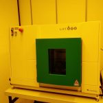
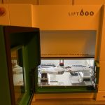
Laser-Induced Forward Transfer System
The laser-induced forward transfer (LIFT) system is utilized to transfer a controlled amount of the donor material onto a receiver substrate by means of laser irradiation. Compared to other printing techniques, LIFT is very competitive due to its material diversity, non-contact, mask-free, nozzle-free nature. It has been utilized to transfer a wide variety of materials like metals, polymers, biomolecules, cells, functional devices, etc.
|
Specifications:
|