Thermal scanning probe lithography (t-SPL) is an emerging technique for rapid prototyping at the nanometer scale. In t-SPL, a heated atomic force microscopy tip is used to pattern a temperature sensitive resist. The fine control over the indentation depth of the tip via an electrostatic potential between the tip and the substrate allows fabrication of grey scale patterns at high precision. These structures can then be transferred into SiOx or Si.
Working Principle
Using the NanoFrazor, a t-SPL tool commercially produced by Swisslitho AG thermal modification of polymer and non-polymeric substrates can be accomplished with nanometer precision at high-speed. In contrast to e-beam lithography, t-SPL can be applied on electron sensitive materials such as InAs nanowires. Another unique feature of NanoFrazor is it’s ability to scan surfaces during patterning. This allows for rapid prototyping.
The basic working principle of thermal patterning is visualized in Figure 1a and 1b. The NanoFrazor canilevers are equipped with two resistive heating elements as shown in Figure 1a). One heater is located above the tip and the second in one of the outer legs. The first heater is used to provide heat to the tip apex via thermal conductance, allowing precise modification of the substrate. The second heater serves as a height sensor which detects changes in the distance between the cantilever and the substrate. During scanning, the thermal height sensing allows fast detection of the patterned topography. More information on the working principle can be found here.
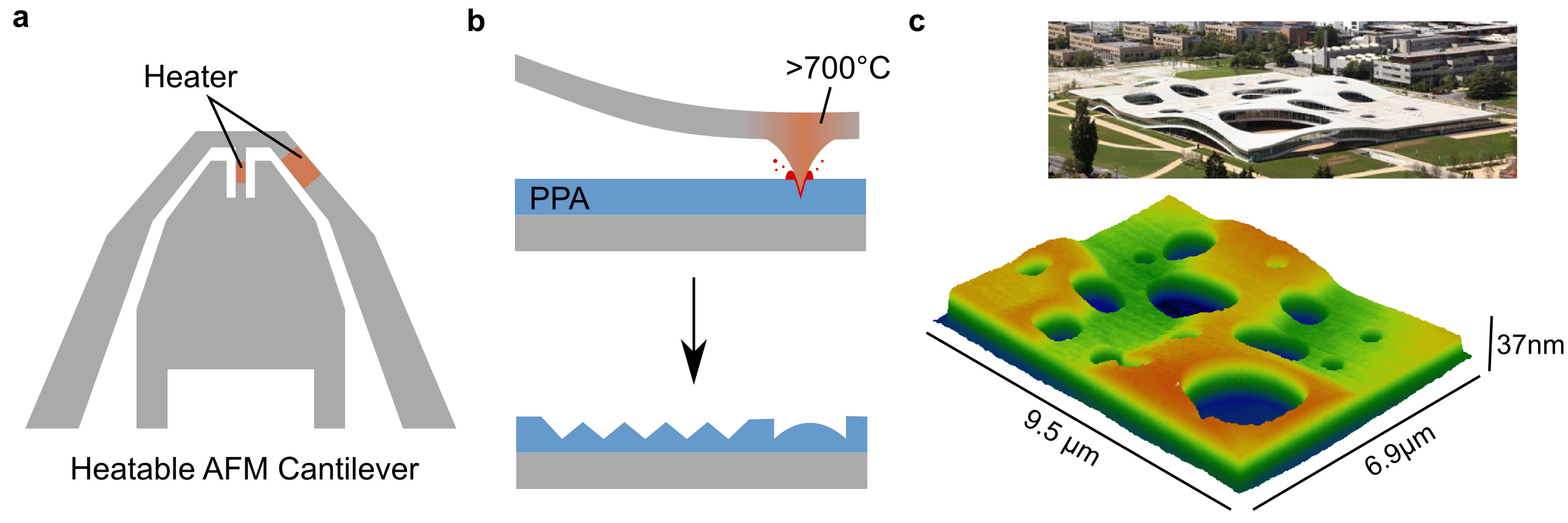
Figure 1b shows the thermal indentation of poly-phthalaldehyde (PPA), a self-amplified resist that decomposes upon exposure to heat (>300°C, ~10µs). By scanning the tip pixel-by-pixel over the surface a 3D topography can be obtained. Figure 1c shows a replica of the Rolex Learning Center at a size of 9.5×6.9µm in PPA, down to the wavy contours of the roof.
Pattern transfer
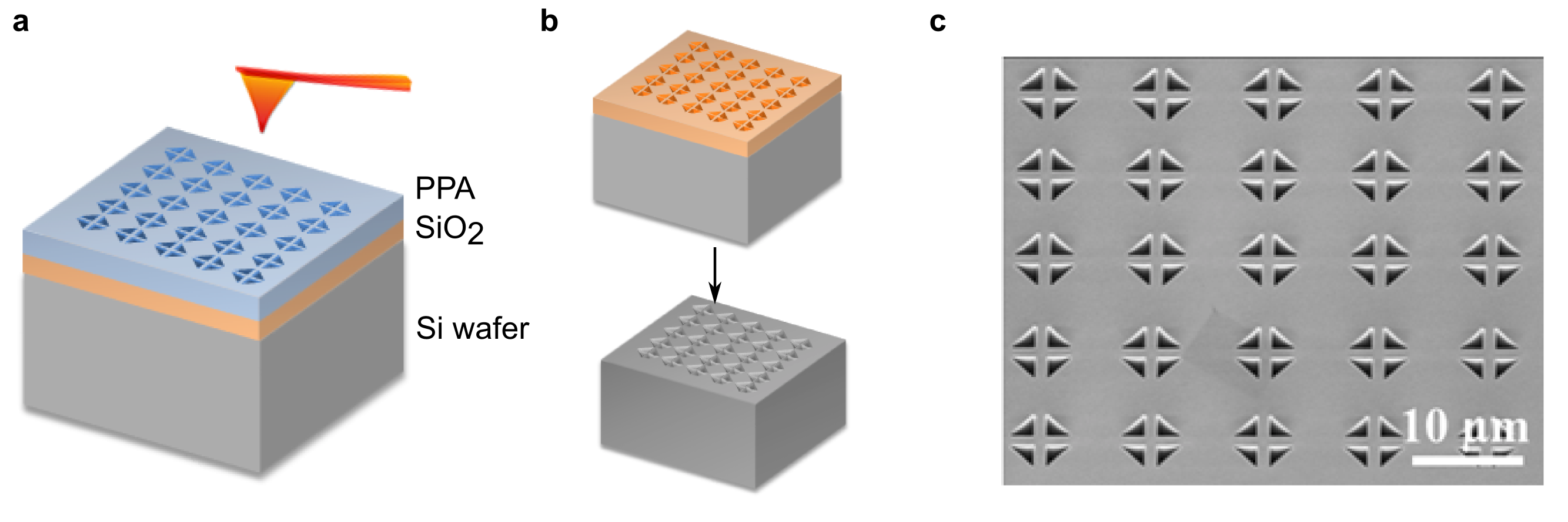
Patterns written into PPA can be transferred into silicon via a dedicated process developped in our lab in collaboration with SwissLitho AG as shown in Figure 2a and 2b. Figure 2c shows a SEM image of structures translated into silicon.
Nanoscale Modification of Supramolecular Glasses
Not only thermal-sensitive resists, but in fact, any material that responds to heat can, in principle, be thermally modified by t-SPL at the nanometer scale.
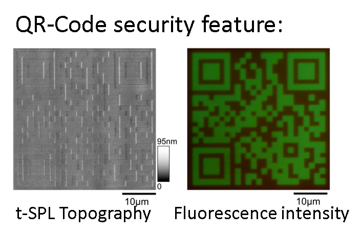
As an example, we modified a fluorescent supramolecular glass to fabricate nano- to microscale security features. This material changes its fluorescence emission wavelength upon heating due to structural changes at the molecular level, which can be observerd using a conventional fluorescence microscope. The results of these modifications can be seen in the below figures. The right figure displays an AFM topography of a modified surface, while the left figure is the results of scanning the surface with the flourescence microscope.
Keywords: thermal scanning probe lithography
Publications
Deterministic grayscale nanotopography to engineer mobilities in strained MoS2 FETs
X. Liu; B. Erbas; A. Conde-Rubio; N. Rivano; Z. Wang et al.
Nature communications. 2024. Vol. 15, num. 1. DOI : 10.1038/s41467-024-51165-4. Edge-Contact MoS2 Transistors Fabricated Using Thermal Scanning Probe Lithography
A. Conde-Rubio; X. Liu; G. Boero; J. Brugger
ACS Applied Materials & Interfaces. 2022. Vol. 14, num. 37, p. 42328 – 42336. DOI : 10.1021/acsami.2c10150. SU-8 cantilever with integrated pyrolyzed glass-like carbon piezoresistor
J. Jang; G. Panusa; G. Boero; J. Brugger
Microsystems & Nanoengineering. 2022. Vol. 8, num. 1, p. 22. DOI : 10.1038/s41378-022-00351-9. Fast turnaround fabrication of silicon point-contact quantum-dot transistors using combined thermal scanning probe lithography and laser writing
C. Rawlings; Y. K. Ryu; M. Rüegg; N. Lassaline; C. Schwemmer et al.
Nanotechnology. 2018. Vol. 29, num. 50, p. 505302. DOI : 10.1088/1361-6528/aae3df. Combination of thermal scanning probe lithography and ion etching to fabricate 3D silicon nanopatterns with extremely smooth surface
Y. Lisunova; J. Brugger
Microelectronic Engineering. 2018. Vol. 193, p. 23 – 27. DOI : 10.1016/j.mee.2018.02.012. Growth of Large-Area 2D MoS2 Arrays at Pre-Defined Locations Using Stencil Mask Lithography
I. Sharma; Y. Batra; V. Flauraud; J. Brugger; B. R. Mehta
Journal of Nanoscience and Nanotechnology. 2018. Vol. 18, num. 3, p. 1824 – 1832. DOI : 10.1166/jnn.2018.14265. Shape Memory Micro- and Nanowire Libraries for the High-Throughput Investigation of Scaling Effects
T. Oellers; D. Koenig; A. Kostka; S. Xie; J. Brugger et al.
Acs Combinatorial Science. 2017. Vol. 19, num. 9, p. 574 – 584. DOI : 10.1021/acscombsci.7b00065. Scanning thermal probe microscope method for the determination of thermal diffusivity of nanocomposite thin films
D. Varandani; K. Agarwal; J. Brugger; B. R. Mehta
Review Of Scientific Instruments. 2016. Vol. 87, num. 8, p. 084903. DOI : 10.1063/1.4960332. Single Superparamagnetic Bead Detection and Direct Tracing of Bead Position Using Novel Nanocomposite Nano-Hall Sensors
M. S. Gabureac; L. Bernau; G. Boero; I. Utke
Ieee Transactions On Nanotechnology. 2013. Vol. 12, num. 5, p. 668 – 673. DOI : 10.1109/Tnano.2013.2266733. Effects of tensile stress on electrical parameters of thin film conductive wires fabricated on a flexible substrate using stencil lithography
M. Frantlović; I. Jokić; V. Savu; S. Xie; J. Brugger
Microelectronic Engineering. 2012. Vol. 98, p. 230 – 233. DOI : 10.1016/j.mee.2012.07.016. CAFM investigations of filamentary conduction in Cu2O ReRAM devices fabricated using stencil lithography technique
B. Singh; B. R. Mehta; D. Varandani; A. V. Savu; J. Brugger
Nanotechnology. 2012. Vol. 23, num. 49, p. 495707. DOI : 10.1088/0957-4484/23/49/495707. High Throughput Nanofabrication of Silicon Nanowire and Carbon Nanotube Tips on AFM Probes by Stencil-Deposited Catalysts
D. S. Engstrom; V. Savu; X. Zhu; I. Y. Y. Bu; W. I. Milne et al.
Nano Letters. 2011. Vol. 11, num. 4, p. 1568 – 1574. DOI : 10.1021/nl104384b. Reliable and Improved Nanoscale Stencil Lithography by Membrane Stabilization, Blurring and Clogging Corrections
O. Vazquez-Mena; K. Sidler; V. Savu; C. W. Park; L. G. Villanueva et al.
IEEE Transactions on Nanotechnology. 2011. Vol. 10, num. 2, p. 352 – 357. DOI : 10.1109/TNANO.2010.2042724. Large arrays of chemo-mechanical nanoswitches for ultralow-power hydrogen sensing
T. Kiefer; A. Salette; G. Villanueva; J. Brugger
Journal of Micromechanics and Microengineering. 2010. Vol. 20, p. 105019. DOI : 10.1088/0960-1317/20/10/105019. An Epoxy Photoresist Modified by Luminescent Nanocrystals for the Fabrication of 3D High-Aspect-Ratio Microstructures
C. Ingrosso; V. Fakhfouri; M. Striccoli; A. Agostiano; A. Voigt et al.
Advanced Functional Materials. 2007. Vol. 17, p. 2009 – 2017. DOI : 10.1002/adfm.200700098. Uniformly Dispersed Deposition of Colloidal Nanoparticles and Nanowires by Boiling
K. Lee; M. Duchamp; G. Kulik; A. Magrez; J. W. Seo et al.
Applied Physics Letters. 2007. Vol. 91, num. 17, p. 173112. DOI : 10.1063/1.2803320. Polymer-based cantilevers with integrated electrodes
S. Mouaziz; G. Boero; R. S. Popovic; J. Brugger
Journal of Microelectromechanical Systems. 2006. Vol. 15, num. 4, p. 890 – 895. DOI : 10.1109/JMEMS.2006.879376. MEMS tools for combinatorial materials processing and high-throughput characterization
A. Ludwig; J. Cao; J. Brugger; I. Takeuchi
Measurement Science and Technology. 2005. Vol. 16, num. 1, p. 111 – 118. DOI : 10.1088/0957-0233/16/1/015. Micromechanical testing of SU-8 cantilevers
M. Hopcroft; T. Kramer; G. Kim; K. Takashima; Y. Higo et al.
Fatigue and Fracture of Engineering Materials and Structures. 2005. Vol. 28, num. 8, p. 735 – 742. DOI : 10.1111/j.1460-2695.2005.00873.x. Submicrometer Hall devices fabricated by focused electron-beam-induced deposition
G. Boero; I. Utke; T. Bret; N. Quack; M. Todorova et al.
Applied Physics Letters. 2005. Vol. 86, num. 4, p. 042503 (3 pages). DOI : 10.1063/1.1856134. Nanomechanical structures with 91 MHz resonance frequency fabricated by local deposition and dry etching
G. Kim; S. Kawai; M. Nagashio; H. Kawakatsu; J. Brugger
Journal of Vacuum Science and Technology B. 2004. Vol. 22, num. 4, p. 1658 – 1661. DOI : 10.1116/1.1761240. Photoplastic near-field optical probe with sub-100 nm aperture made by replication from a nanomould
G. Kim; B. Kim; E. Ten Have; F. Segerink; N. Van Hulst et al.
Journal of Microscopy. 2003. Vol. 209, num. 3, p. 267 – 271. DOI : 10.1046/j.1365-2818.2003.01134.x. Surface Modification With Self-Assembled Monolayers for Nanoscale Replication of Photoplastic MEMS
G. M. Kim; B. J. Kim; M. Liebau; J. Huskens; D. N. Reinhoudt et al.
Journal of Microelectromechanical Systems. 2002. Vol. 11, num. 3, p. 175 – 181. DOI : 10.1109/JMEMS.2002.1007395.