Our aim is to push the limits of shadow-mask surface pattering to reach smaller structures (> 50 nm) and to upscale to larger substrates. We strive to find solutions to challenges such as aperture clogging, gap induced blurring and surface diffusion. Further we develop a so-called dynamic stencil tool where the shadow mask moves with respect to the substrate.
Stencil lithography
 |
 |
 |
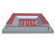
| The stencil is fabricated and aligned to the substrate |
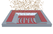
Both substrate and stencil are placed into the evaporator |
The stencil is removed, leaving the patterned substrate |
Stencil lithography is a high resolution shadow-mask technique used for structuring surfaces at the micro and nanometer scales. It is a one-step technique that eliminates resist-related processing steps, common otherwise in standard lithography. A stencil (membrane with apertures) is placed (aligned if necessary) and clamped to a substrate. The clamped set is placed in an evaporator and material is despotied through the stencil’s apertures onto the substrate.
Stencil lithography is applicable to deposition, etching and implantation.
Dynamic stencil lithography consists of the relative motion of the stencil to the substrate during deposition or in between deposition steps. This allows the in-situ fabrication of multi-material, multi-layer micro- and nanopatterns.
Keywords: stencil, stencil lithography
Publications
Selector‐Free 16 × 16 CrOX/TiO2‐Based Memristor Array for Synaptic Dynamics and LTP/ LTD Emulation: Experimental–Computational Correlation
P. Pham; T. Tran; T. Vo Van Anh; T. D. Nguyen; J. Brugger et al.
Advanced Functional Materials. 2025. DOI : 10.1002/adfm.202516695. Laser-Induced Forward Transfer of SU-8 Microdisks as Carriers of Metallic Microdevices
Z. Yang; G. Boero; R. Widmer; J. Michler; R. Pero et al.
Journal of Microelectromechanical Systems. 2024. DOI : 10.1109/JMEMS.2024.3487248. Nanobridge Stencil Enabling High Resolution Arbitrarily Shaped Metallic Thin Films on Various Substrates
Y-C. Sun; G. Boero; J. Brugger
Advanced Materials Technologies. 2022. DOI : 10.1002/admt.202201119. Stretchable Conductors Fabricated by Stencil Lithography and Centrifugal Force-Assisted Patterning of Liquid Metal
Y-C. Sun; G. Boero; J. Brugger
ACS Applied Electronic Materials. 2021. Vol. 3, num. 12, p. 5423 – 5432. DOI : 10.1021/acsaelm.1c00884. Biodegradable Frequency‐Selective Magnesium Radio‐Frequency Microresonators for Transient Biomedical Implants
M. Rüegg; R. Blum; G. Boero; J. Brugger
Advanced Functional Materials. 2019. Vol. 29, num. 39, p. 1903051. DOI : 10.1002/adfm.201903051. Growth of Large-Area 2D MoS2 Arrays at Pre-Defined Locations Using Stencil Mask Lithography
I. Sharma; Y. Batra; V. Flauraud; J. Brugger; B. R. Mehta
Journal of Nanoscience and Nanotechnology. 2018. Vol. 18, num. 3, p. 1824 – 1832. DOI : 10.1166/jnn.2018.14265. Optical Antenna-Based Fluorescence Correlation Spectroscopy to Probe the Nanoscale Dynamics of Biological Membranes
P. Winkler; R. Regmi; V. Flauraud; J. Brugger; H. Rigneault et al.
The Journal of Physical Chemistry Letters. 2018. num. 9, p. 110 – 119. DOI : 10.1021/acs.jpclett.7b02818. Shape Memory Micro- and Nanowire Libraries for the High-Throughput Investigation of Scaling Effects
T. Oellers; D. Koenig; A. Kostka; S. Xie; J. Brugger et al.
Acs Combinatorial Science. 2017. Vol. 19, num. 9, p. 574 – 584. DOI : 10.1021/acscombsci.7b00065. Growth Of Organic Semiconductor Thin Films with Multi-Micron Domain Size and Fabrication of Organic Transistors Using a Stencil Nanosieve
P. Fesenko; V. Flauraud; S. Xie; E. Kang; T. Uemura et al.
ACS Applied Materials & Interfaces. 2017. Vol. 9, num. 28, p. 23314 – 23318. DOI : 10.1021/acsami.7b06584. Scanning thermal probe microscope method for the determination of thermal diffusivity of nanocomposite thin films
D. Varandani; K. Agarwal; J. Brugger; B. R. Mehta
Review Of Scientific Instruments. 2016. Vol. 87, num. 8, p. 084903. DOI : 10.1063/1.4960332. Exploring Nanoscale Electrical Properties of CuO-Graphene Based Hybrid Interfaced Memory Device by Conductive Atomic Force Microscopy
B. Singh; B. Mehta; D. Varandani; A. V. Savu; J. Brugger
Journal of Nanoscience and Nanotechnology. 2016. Vol. 16, num. 4, p. 4044 – 4051. DOI : 10.1166/jnn.2016.10713. Fabrication of complex oxide microstructures by combinatorial chemical beam vapour deposition through stencil masks
E. Wagner; C. S. Sandu; S. Harada; G. Benvenuti; V. Savu et al.
Thin Solid Films. 2015. Vol. 586, p. 64 – 69. DOI : 10.1016/j.tsf.2015.04.021. Application of stencil masks for ion beam lithographic patterning
S. Brun; V. Savu; S. Schintke; E. Guibert; H. Keppner et al.
Nuclear Instruments and Methods in Physics Research Section B: Beam Interactions with Materials and Atoms. 2013. Vol. 306, p. 292 – 295. DOI : 10.1016/j.nimb.2012.12.064. Stencil-Nanopatterned Back Reflectors for Thin-Film Amorphous Silicon n-i-p Solar Cells
C. Pahud; V. Savu; M. Klein; O. Vazquez-Mena; F-J. Haug et al.
Ieee Journal Of Photovoltaics. 2013. Vol. 3, num. 1, p. 22 – 26. DOI : 10.1109/Jphotov.2012.2213583.