Introduction
Polymer-derived ceramics (PDCs) are a class of ceramics that can be prepared, without any additives, by the thermal handling of appropriate precursors in an inert or reactive atmosphere. PDCs present exceptional properties that include stability towards oxidation and corrosion, as well as crystallization and creep resistance up to very high temperatures.[1]
In our group, we research on the materials’ property improvement and tuning as well as suitable shaping techniques targeting applications in the fields of MEMS and biomedical implants. For the latter, we also investigate the biocompatibility and electrochemical behavior.
Shaping
PDCs can be applied as thin coatings or shaped by casting as well as (stereo)lithography. We focus on developing new (micro)mold fabrication strategies achieving parts with complex shapes and high precision. For this, established photolithography methods are utilized, optimized, and combined in CMi. Resulting molds are further processed, e.g. adding features by two photon polymerization (2PP) or applying coatings for improved wettability and demoldability before casting the precursor inside. A schematic overall summary is given in Figure 1.
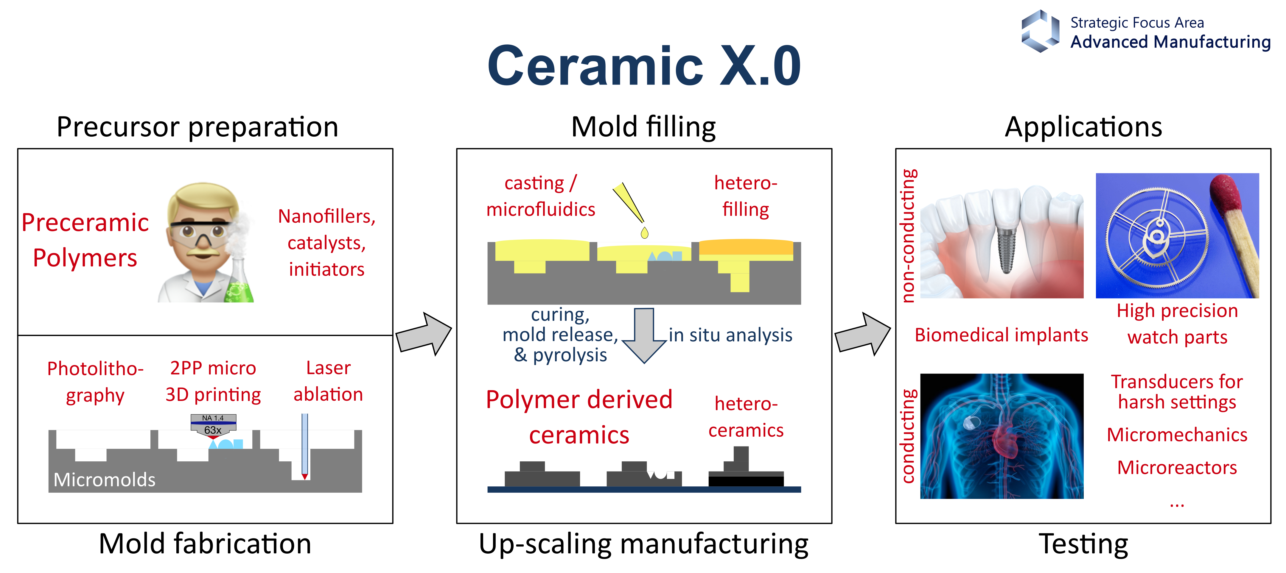
Figure 1: Fabrication overview of complex shape PDC microparts with custom properties and potential applications.
Material
The PDC processing route allows multiple ways of adjusting the resulting ceramics’ composition and microstructure and hence mechanical or functional properties. Starting from different kinds of so-called preceramic polymers (PCPs) such as polysiloxanes or polysilazanes, fillers, catalysts, or initiators can be added. By means of thermal treatment or UV-irradiation, the liquid precursors transform into fused greenbodies as they crosslink (Figure 2). Subsequent pyrolysis, typically in inert atmosphere at temperatures between 700°C and 1600°C, transforms the greenbodies into inorganic (polymer-derived) ceramic material such as silicon carbonitride (SiCN) or silicon oxycarbide (SiOC). The choice of the related parameters such as atmosphere, heating and cooling rate, as well as peak pyrolysis temperature and dwell time determines the resulting characteristics. A strategy to increase the PDC’s electrical conductivity for example is the addition of conductive filler phase (e.g. carbon) and higher pyrolysis treatment to establish a C percolation network in the material.
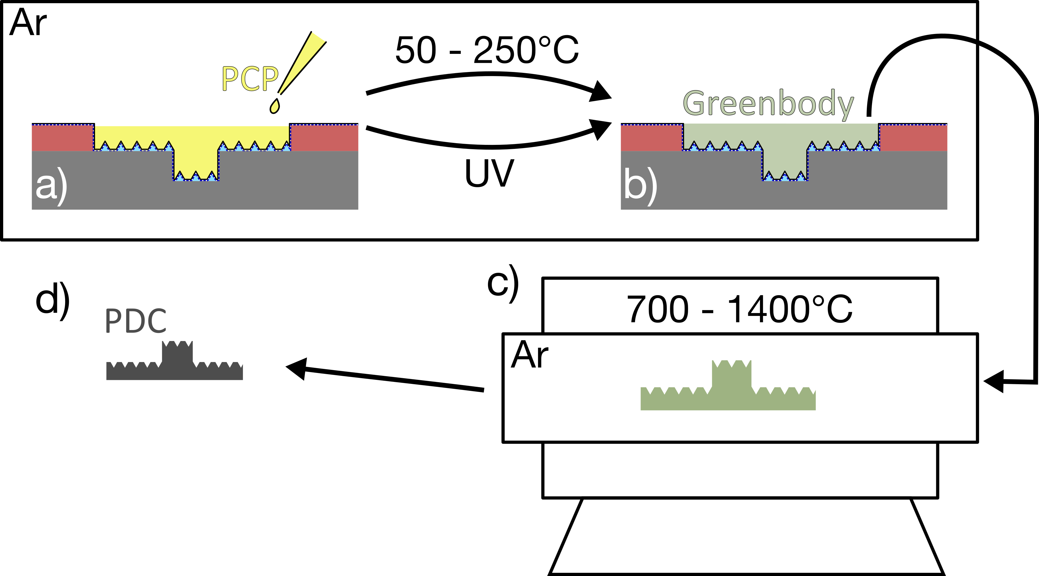
Figure 2: Schematic PDC processing route: a) Mold filling in protective atmosphere, b) UV or thermal curing and greenbody demolding, c) high temperature pyrolysis, d) final PDC micropart.
C-MEMS
Other selected polymers (such as the epoxy-based photoresist SU-8) can be converted into glassy carbon (GC) by inert gas pyrolysis at temperatures around 900°C. While this material family allows a smaller range of property controllability and typically lower mechanical properties compared to PDCs, its strength is the extraordinary shape control by direct photolithography. In this way, extremely precise 2D or 2.5D MEMS and microparts can be produced in GC. Being electrically conductive, a range of applications such as electrodes and sensors is investigated.
Biocompatibility and electrochemistry
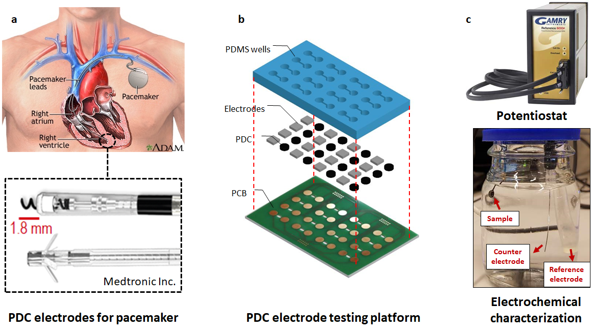
Figure 3. a) Schematics for pacemaker electrodes b) PDC electrode testing platform c) Setup for electrochemical characterization of PDCs
A pacemaker is a surgically implantable electronic device that stimulates the heart muscle to maintain an adequate heartbeat. In the pacemaker, the electrode is designed to be fixed to the cardiac tissue to deliver electrical pulses. The state-of-the-art pacemaker electrode is metal electrodes coated with Pt or TiN (Figure 3a). In our research, we apply PDCs as pacemaker electrode instead of metal to minimize foreign body reaction. A PDMS-based testing platform is fabricated to evaluate the PDC electrode and biocompatibility (Figure 3b). Also, the electrochemical properties of the PDC electrodes are characterized by the impedance spectroscopy and cyclic voltammetry (Figure 3c).
[1] E. Ionescu, “Polymer-derived ceramics“, in Ceramics Science and Technology, Set (R. Riedel and I.-W. Chen, eds.), pp. 457–500, Wiley-VCH Verlag GmbH & Co. KGaA, Weinheim, Germany, 2013.
Keywords: ceramics