Self-sensing piezoresistive cantilevers for atomic force microscopy are an alternative to the optical beam deflection (OBD) readout system. They make use of the piezoresistive effect of silicon to detect deflection-induced strain at the cantilever surface and present the advantage of a much better usability, as no laser alignment is required. However, while they have shown similar performance to OBD in terms of low noise topography imaging, piezoresistive cantilevers cannot compete with the laser readout in force sensing applications, where soft cantilevers are required. Indeed, silicon cantilevers have to be made long and thin to reach low spring constants; compared to short and thick cantilevers, this signifies a much lower strain at the cantilever surface, and thus a drastic reduction of piezoresistive readout sensitivity. For force imaging of biological samples, an additional issue lies in the fact that the cantilevers are not suited for applications in liquids, as the sensor readout electronics are usually exposed.
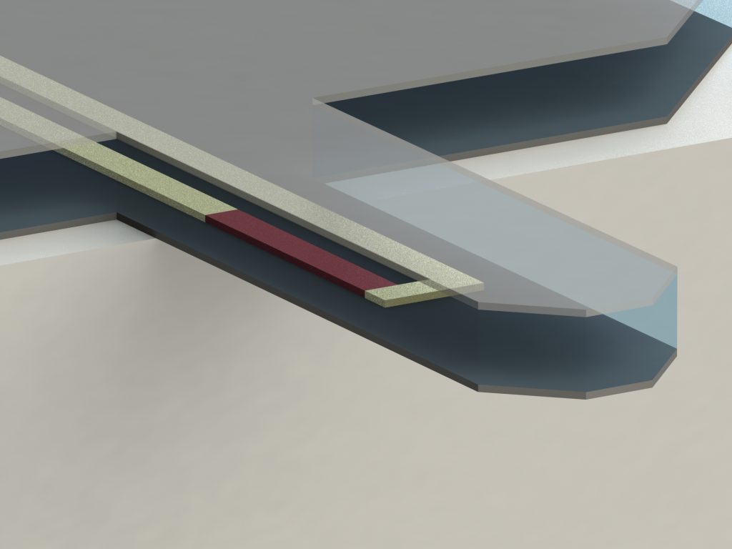
We have developed a new device (Figure 1) to tackle these issues: a trilayer cantilever, made of a polymer core, piezoresistive polysilicon strain sensors and a hard shell encapsulation. For identical spring constants, such cantilevers can be made shorter and thicker than their silicon counterparts, presenting higher sensitivity. In addition, the shell isolates the sensors from the environment, making the cantilevers inherently fluid compatible.
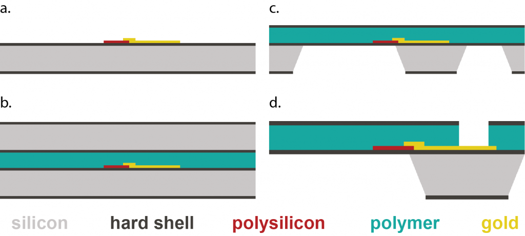
The fabrication process is a mix between traditional and alternative microfabrication techniques, hence the term ‘hybrid MEMS’. We start by patterning the electronic readout on top of a thin film that will form the hard shell. This is done through a series of lithography, etching and lift-off steps (Figure 2, a). The wafer is then coated with a polymer and bonded to a second wafer (b). The trilayer structure, consisting of two hard shell layers and a polymer core is the released through wet-etching (c). Finally the device is structured through lithography and dry-etching (d).
The trilayer devices have many advantages and pave the way for a variety of self-sensing applications in AFM and other fields. The features of the process includes the following:
- Self-sensing with high sensitivity
- Fluid compatibility
- Robust and variable process for various device types
- Possibility of adding coatings, for example for a metallic tip connection
While this process has only been used to fabricate fluid compatible self-sensing cantilevers, it can be adapted in many ways to fabricate devices for a large number of applications. The project is ongoing, with the goal to establish the trilayer technology as new benchmark MEMS fabrication technique.