Are you passionate about the nanoscale and its gateway, the AFM? Would you like to make use of your microfabrication skills to work on cutting-edge MEMS technology? Are you interested in observing biology at its smallest scale? Or do you want to push the imaging speeds of AFM through innovative control?
If any of those apply to you, then LBNI is the lab for your semester or master project!
Development of AFM cantilevers
Semester / Master project
Introduction
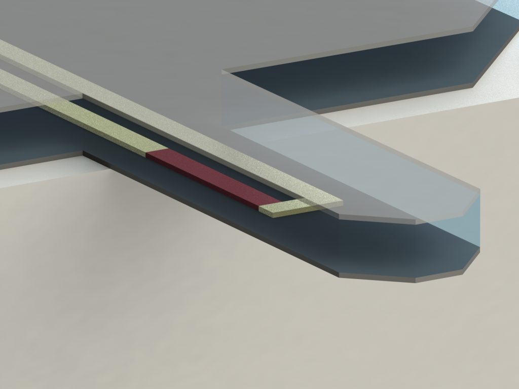
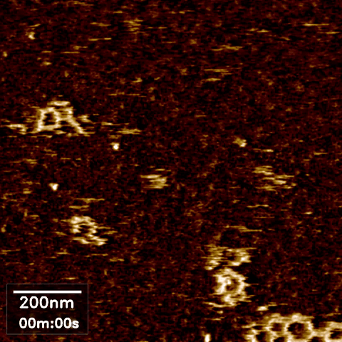
Two primary research goals in AFM are increasing the imaging speed and improving the ease of use to expand the potential range of applications. To address these objectives, we have started developing polymer based [1], self-sensing cantilevers [2] to improve the mechanical bandwidth of the cantilevers and be able to use a simple electrical readout to detect the deflection of the cantilever. These self-sensing devices are a promising replacement for the current state of the art cantilevers that are used with a complex laser based optical readout. You will find more information about our devices here.
Scope
While we are able to fabricate such cantilevers with high yield, we are now looking to improve them and adapt them for specific AFM applications. To help us do so, we are looking for highly motivated students who want to learn multidisciplinary skills. In joining us, you will be collaborating with a PhD student and you will get to know all about the fabrication of MEMS devices the EPFL cleanrooms, the CMi. In addition you will learn how to perform self-sensing AFM imaging. A successful completion will be subject to publication.
Interested? The different research axes are listed below!
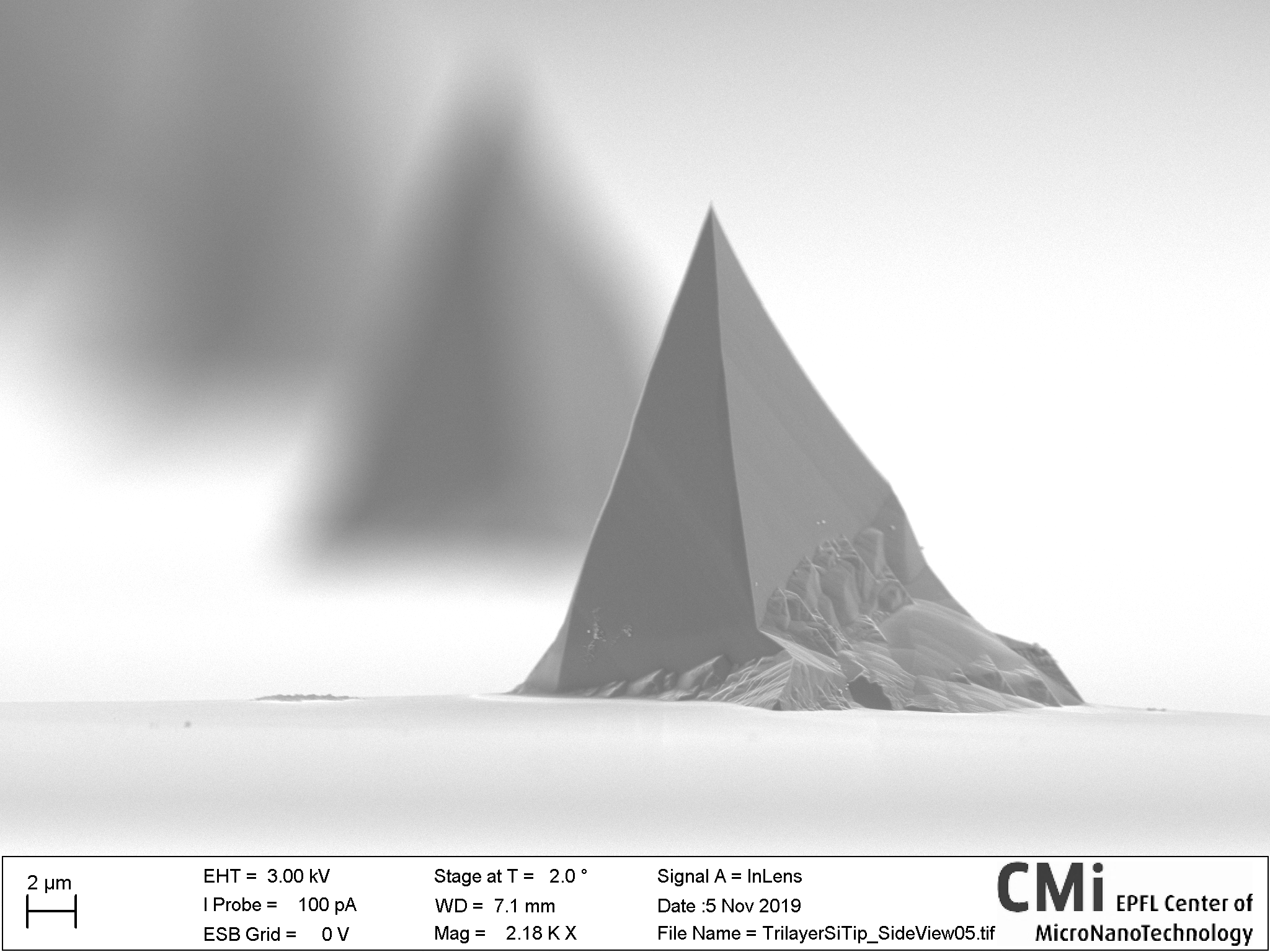
Our current cantilevers have no tips and we are forced to add them one by one manually, which is very time consuming. To address this problem, you will be charged with developing a process to add tips onto our cantilevers directly during their fabrication.

In various AFM techniques, conductive tips are used to probe the surface. Since our cantilevers have embedded electronics, we experience cross-talk effects between them and the tip-connection. You will have to modify the process flow such as to add a grounded metal connection between the two signal lines, then use the fabricated cantilevers for electrical measurements in AFM.
We currently use the piezoresistive effect in poly-silicon to sense the deflection of our cantilevers. This material has a gauge factor of about 30. There are other materials, for instance single crystal silicon, that exhibit much higher gauge factors. You will be charged to modify the current process flow such as to replace the poly-silicon with single crystal silicon sensors.
What you will learn
- Cleanroom fabrication skills like photolithography, dry/wet etching, thin film deposition
- Creative thinking to find ways of manufacturing complex devices with standard microfabrication techniques
- Layout design for photolithography
- AFM imaging
Desired skills
- Fluency in English
- Autonomy
- Enjoys learning and facing new challenges
- Theoretical knowledge of microfabrication techniques (ex: fundamentals of microfabrication, materials and technology of microfabrication, MEMS practicals)
References
[1] Adams, Jonathan D., et al. “Harnessing the damping properties of materials for high-speed atomic force microscopy.” Nature nanotechnology (2015).
[2] Fantner, G. E., Adams, J. D. & HOSSEINI, N. Multilayer mems cantilevers. (2018).
Contact

At LBNI, we develop instruments at the forefront of nanoscale biology and one of our key strengths is instrumentation for atomic force microscopy (AFM). We develop high-speed AFM to push the current limits of imaging speeds. We believe that open hardware is the way forward to share the instruments and technologies that we develop, to the wider scientific community.
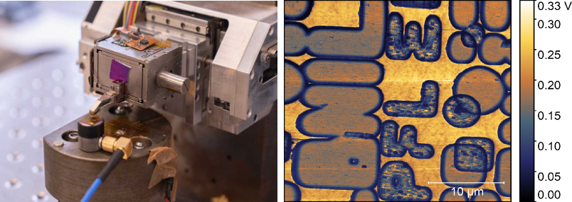
In the age of correlative microscopy, combining two modalities of microscopy techniques is fascinating. However, such combinations are to be facilitated to take the most advantage of this combination. Combining an atomic force microscope (AFM) and a scanning electron microscope (SEM) (Crossbeam 550L FIB/SEM system), allows us to have sub-nanometer resolution of an AFM with fast scan imaging of the SEM in challenging samples. However, beyond imaging AFM can help us achieve contrast based on different mechanical characteristics of materials which can be combined with the chemical contrast achieved by SEM’s backscattered detectors.
Contact resonance (CR) measurements are a very unique of set of surface and subsurface imaging where the tip-sample contact is ultrasonically excited at a specified frequency and the amplitude and phase of the contact resonance is monitored. This contact resonance being sensitive to the sample’s local mechanical properties, CR-AFM can help us map the various mechanical properties of the sample. Varying the force (setpoint) for the contact mode imaging, this method can be used to perform sub-surface imaging which can complement the SEM’s in depth backscattered analysis.
We aim to facilitate these CR-AFM measurements in our AFM which operates inside the SEM chamber. To achieve this, we need to facilitate sending a signal to the sample inside the SEM and use frequency tracking with a lock-in amplifier to discern the different material present below the surface and complement it with SEM imaging.
What you will learn:
- AFM (CR-AFM) imaging and SEM imaging
- Interpret material contrast based on frequency tracking
- Use of Lock-in amplifier and instrumentation for vacuum technology
Desired skills:
- Fluency in English
- Ability and willingness to learn new skills independently
Contact


Semester Master Project
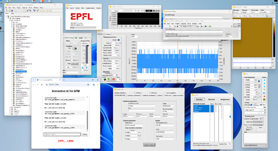
As part of our OpenSPM initiative, with multiple instruments already installed in labs and companies around the globe, we recently created a simple proof-of-concept AI chatbot. This work represents a first step towards making advanced SPM instrumentation more intuitive and accessible. One of the core goals is to allow researchers to control the instrument using natural human language instead of writing code. In this approach, the chatbot translates conversational instructions into Python commands that interact with our API, which already provides programmatic access to all core AFM functions. This enables users to define and execute even complex experimental tasks in plain language, while the AI handles the translation into precise code.
The current prototype demonstrates this capability for simple actions such as setting imaging parameters or initiating scans. The next steps are to expand the chatbot’s scope, improving its accuracy through retraining, and testing it under realistic experimental conditions. Another important objective is to explore how AI can help design and automate experimental workflows, going beyond single tasks to the orchestration of multi-step procedures. Ultimately, this project aims to create an AI-powered assistant that not only lowers the technical barrier to operating AFMs but also enhances flexibility, usability, and efficiency. By bridging human language and instrument control, it opens the possibility of more creative and adaptive experimental design, empowering researchers across different backgrounds to take full advantage of OpenSPM systems.
What you will learn
- AFM/SICM imaging and corresponding parameters.
- Software development including chatbot
- Applied machine learning and AI training
Desired skills
- Fluency in English.
- Python is mandatory. Java is a plus.
- General knowledge of AI training and machine learning
- Ability and willingness to pick up new skills independently.
[1] https://www.epfl.ch/labs/lbni/spm-controller-software/
Contact


Introduction
Atomic force microscopy (AFM) can take high-resolution images of nanoscale objects in various environments. Since conventional AFM imaging is too slow to capture dynamic processes of, for example, behavior and interaction of biomolecules, high speed AFM (HS-AFM) has been developed by optimizing the software and hardware in the instrument for fast scanning.
AFM images often require some post-processing in an open source software called Gwyddion. Data obtained from AFM imaging software Nanoscope can be directly imported, processed to flatten, remove lines and scars, and define the zero-level and contrast, then exported as a common image format such as jpeg. However, our existing software packages were not designed to handle the volume of data produced during HS AFM imaging, where we obtain hundreds of images per experimental run.
Scope
In high speed AFM imaging, we obtain a large quantity of images, which would take a significant amount of time to process with Gwyddion one by one. We are therefore looking for an interested Masters or semester project student to develop more efficient or automated AFM image processing for converting a series of HS-AFM images from the same experiment to a video format.
Project Task
Your task will be to design and test and a plugin for Gwyddion to efficiently process HS AFM data into videos.
What you will learn
- AFM imaging
- AFM image processing
- Interface with open source AFM image processing software
Desired skills
- Fluency in English
- Coding basics (Python)
- Ability and willingness to pick up new skills independently