Laboratory LBNI and LBEN have developed system for nanopore-based label-free single-molecule sensor – scanning ion conduction spectroscopy (SICS)1, Fig 1A. It utilizes a glass nanopore mounted on a three-dimensional nano positioner to spatially select molecules tethered on a glass surface for controlled translocations. This technique grants us the ability to actively choose specific regions of interest on the DNA and scan molecules a predetermined number of times and at a controlled velocity, Fig 1B.
LBNI group has a wealth of experience and expertise developing a wide range of instruments at the forefront of nanoscale biology. One of our key strengths is instrumentation for scanning probe microscopy (SPM) techniques such as scanning ion conduction microscopy (SICM). In SPM instruments, the controller plays a crucial role as servers as a control hub for all the sensors and actuators used in the system. In our lab, we have designed and developed a modular SPM controller (hardware and software) that provides open access at all levels, delivering at the same time research-grade performance in an open hardware philosophy, with several users around the world2. This gives the flexibility to adapt the controller to any setup and needs, making it easier to add new functionalities or devices. Thus, this controller has been deployed for various SPM research projects, including high-speed AFM, scanning electron microcopy (SEM), and other novel techniques.
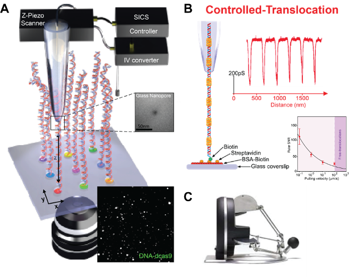
We are offering a semester/master project or an internship opportunity to work on implementing use of Omega.x haptic device (Fig 1c) for sensing DNA analytes with nanometer-sized capillary. Manipulation in XYZ, with the right routines showing how close the tip is to the surface, would be programmed in LabView software. To achieve this, it is vital to optimize the communication architecture to reach fast controller/haptic device update rate (> 1 kHz), and to design a well-integrated human interface to facilitate its usability.
What you will learn
- SICS sensing and data processing
- Interface with open-source SPM software control.
- The principles of nano-manipulation based on Omega.x haptic devices.
Desired skills
- Fluency in English.
- LabView programming experience.
- Ability and willingness to pick up new skills independently.
Reference:
- Leitao, S. M. et al. Spatially multiplexed single-molecule translocations through a nanopore at controlled speeds. Nat. Nanotechnol. 18, 1078–1084 (2023).
- https://www.epfl.ch/labs/lbni/spm-controller-software/

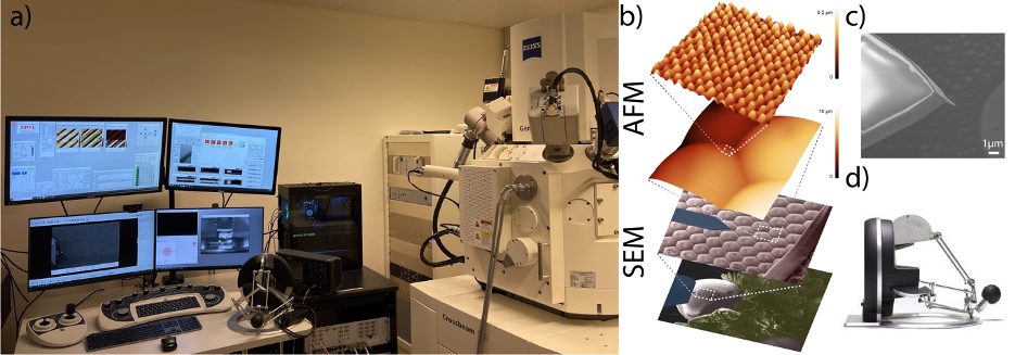
Our laboratory (LBNI) has a wealth of experience and expertise developing a wide range of instruments at the forefront of nanoscale biology. One of our key strengths is instrumentation for scanning probe microscopy (SPM) techniques such as atomic force microscopy (AFM). In SPM instruments, the controller plays a crucial role as servers as a control hub for all the sensors and actuators used in the system. In our lab, we have designed and developed a modular SPM controller (hardware and software) that provides open access at all levels, delivering at the same time research-grade performance in an open hardware philosophy, with several users around the world [1]. This gives the flexibility to adapt the controller to any setup and needs, making it easier to add new functionalities or devices. Thus, this controller has been deployed for various SPM research projects, including high-speed AFM, scanning electron microcopy (SEM), and other novel techniques. Recently, we have implemented an AFM inside of a CrossBeam 550L FIB/SEM system (AFSEM) (Fig 1a), where we combined the sub-nanometer resolution of an AFM with a wide range area and fast scan imaging of the SEM, enabling the imaging of challenging samples (Fig 1b).
We aim to use the nanometer size cantilever tip as a nano-manipulator tool (Fig 1c), controlled by an Omega.x haptic device (Fig 1d), programing in LabView the required routines to control the cantilever XYZ position. To achieve this, it is vital to optimize the communication architecture to reach fast controller/haptic device update rate (> 1 kHz), and to design a well-integrated human interface to facilitate its usability. This device will also serve as a tool for the functional understanding of AFM.
What you will learn:
- AFM and SEM imaging and image processing.
- Interface with open-source SPM software control.
- The principles of nano-manipulation based on Omega.x haptic devices.
Desired skills:
- Fluency in English.
- LabView programming experience.
- Ability and willingness to pick up new skills independently.
[1] https://www.epfl.ch/labs/lbni/spm-controller-software/
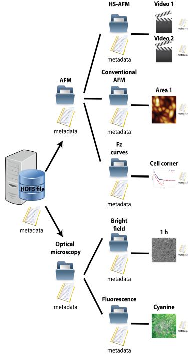
Open-source data schemes are becoming increasingly important for scientific data storage. They enable sharing of software, data, and knowledge at early phases in the scientific process, as well as proper long-term preservation storage. In this project, we aim to implement the HDF5 and USID open standards on an already well-established ORD worldwide project at LBNI: the Open-Source SPM controller [1]. Its current file scheme presents several weaknesses(maximum file size, metadata attachment, long term data curation, etc.) that we intend to overcome with those modern standards. Thus, the implementation of this scheme will enable the access to a lively open software ecosystem called Pycroscopy, where the Open-Source SPM project will take advantage of all the functionalities and tools already existing on that ecosystem based on the HDF5 and USID open standards.
In the frame of this project, we will need to design the different data structures represented via the USID model for the different techniques involved on the Open-Source SPM controller (Fig. 1): AFM, spectroscopy- AFM, HS-AFM, SICM, SEM, AFSEM, SNOM, optical microscopy and fluorescence. We will define the adequate USID structure to fulfil the different data generated by the previously enumerated techniques. At this point, it is crucial to design a proper metadata template for each technique, that can contain all the relevant information. After, all the USID designed schemes that will generate the HDF5 files from the acquired data on the Open-Source SPM controller will be coded using C/C++ language, generating Dynamic-link libraries (DLLs), which will be directly embedded on the LabView code that controls the Open-Source SPM controller.
What you will learn:
- AFM imaging and image processing.
- Interface with open-source SPM software control.
- Knowledge of the modern and open HDF5-USID scheme for advanced data storage.
Desired skills:
- Fluency in English.
- C/C++ programming experience, LabView knowledge is a plus.
- Ability and willingness to pick up new skills independently.
[1] https://www.epfl.ch/labs/lbni/spm-controller-software/
Contact
Microfluidic chip for selective delivery of bacterial cells
Master project
Design and implementation of a microfluidic device that sorts and delivers bacterial cells on demand. For the design, standard cleanroom fabrication technology will be used. The devices are made on silicon wafers using photolithography and dry etching. The final device will be out of soft polymer (e.g. PDMS). Similar devices have already been fabricated [1]; the goal will be to implement this into an already existing microfluidic system. You will be in charge of the design and fabrication of the microfluidic chip. After the fabrication, you will use polymer beads and yeast cells for the proof of principle of the cell sorting architecture of the microfluidic chip. The final goal will be to sort and selectively deliver rod-shaped bacteria on a microfluidic chip assembly for atomic force analysis.
Recommended background
- Basic knowledge in cleanroom fabrication
- Basic knowledge in CAD design
In this project you will:
- Design a microfluidic chip (with e.g. CleWin)
- Fabricate the microfluidic chip using standard cleanroom fabrication techniques
- Design the interface to the microfluidic chip with CAD software (e.g. Solidworks)
- Test the fabricated microfluidic chip setup with biological samples
Contact
References
[1] Monolithic microfabricated valves and pumps by multilayer soft lithography, Unger M et al., Science, 2000.
Bacteria analysis with atomic force microscopy
Master or Semester project
Using a developed microfluidic device for the immobilization of bacteria, the goal will be to analyze rod-shaped bacteria under the influence of different environmental conditions. In particular, by mimicking conditions in the gastrointestinal tract, bacteria (e.g. Escherichia coli and Bacillus subtilis) will be exposed to specific antibiotics. With the atomic force microscope (AFM) we will observe the changes on the surface of bacteria (and mechanical properties if master project). The experiment setup consists of an atomic force microscope with an inverted fluorescence microscope. The final goal is to determine whether there are and how much in particular, the conditions in the gastrointestinal tract influence the bacterial susceptibility to antibiotics (e.g. antimicrobial peptides).
Recommended background
- Basic knowledge in microbiology
In this project you will:
- Gain experience with AFM imaging on biological samples
- Use a microfluidic system together with a fluorescence microscope and AFM
- Use the obtained data for advanced analysis of bacteria under specific conditions
Contact
Fabrication of tri-layer cantilevers
Master project
Two primary research goals in AFM are increasing the imaging speed and improve ease of use to expand the potential range of applications. We are working on the fabrication of polymer based [1], self-sensing cantilevers to improve the mechanical bandwidth of the cantilevers and make a simple electrical readout to detect the deflection of the cantilever. Such a self-sensing technique is a promising replacement for the complex laser based optical readout.
We offer a project for students for both semester and master projects in the filed of micro-engineering. The student task will be the optimization of the signal to noise ratio to improve the electrical readout. This will be in collaboration with a PhD student where you will learn how to perform self-sensing AFM imaging in air and liquid. We are looking for a motivated student who wants to learn multidisciplinary skills. A successful completion will serve as a template for future experiments and can be applied to different aspects of MEMS fabrication and biosensors.
In this project you will learn:
- Clean room fabrication skills like photolithography, dry/wet etching, thin film deposition, etc.
- Low noise measurement techniques
- AFM imaging
References
[1] Adams, Jonathan D., et al. “Harnessing the damping properties of materials for high-speed atomic force microscopy.” Nature nanotechnology (2015).
Contact
[email protected]
[email protected]
Fabrication of nm-resolution and μm-range position sensor
Master project
Many companies and research groups are interested in fabrication of sensitive, low noise, high bandwidth and compact position sensors. Such a strain sensor has several applications in research and industry where positioning with nm-resolution is required. Recently sidewall doped piezoresistor has shown attractive properties upon their fabrication techniques and applications.
We offer a project for students for both semester and master projects in the filed of micro-engineering. The proposed project is linked to our ongoing development of strain sensors. The student task will be to further develop these novel sensors in collaboration with our industrial partner. We are looking for a motivated student who wants to learn multidisciplinary skills. At the end of this project you will learn micro-fabrication skills like lithography, dry/wet etching, thin film deposition, etc. as well as measurement techniques. A successful completion will serve as a template for future experiments and can be applied to different aspects of MEMS fabrication.
In this project you will learn:
- Clean room fabrication skills like photolithography, dry/wet etching, thin film deposition, etc.
- Low noise measurement techniques
- Implementation of the closed loop systems
References
[1] Hosseini, N., et al. “A monolithic MEMS position sensor for closed-loop high-speed atomic force microscopy.” Nanotechnology 27.13 (2016): 135705.
Contact
Design and fabrication of a quadrature interferometric detection for video rate material atomic force microscopy on ultra-small cantilevers
Master project
Atomic force microscopy relies heavily on the calibration of the used cantilever probes. Traditionally the cantilever motions are detected by optical beam deflection. Using an interferometric detection scheme the cantilever motion is directly compared to the wavelength of light, enabling an extremely low noise detection at a bandwidth of multiple megahertz. Additionally, the spot can be made extremely small allowing for the readout of arbitrary MEMS and NEMS cantilevers. Using this, highly accurate nanoscale mechanical property measurements are enabled.
In this project you will:
- Learn about state of the art optical systems and design of optics assemblies.
- Gain experience in designing and manufacturing mechanical parts using computer aided design.
- Get introduced to modern high-frequency atomic force microscopy techniques for mechanical characterization at the nanoscale
Contact
Combining high resolution optical microscopy with high-speed AFM
Scanning confocal microscopy has become one of the most powerfull tools in optical microscopy for imaging the inside of cells. Atomic Force Microscopy (AFM) is unsurpassed in it’s capability to resolve nanometer sized features on the surface of living systems in physiological solution. A combination of these two techniques will allow a seamless characterization of cell surface phenomena with phenomena occuring on the inside of a cell.
We have developped specialized high speed Atomic Force Microscopes which can take images up to three orders of magnitude faster than conventional AFMs. This allows us to image dynamic processes in real time. This masters project is part of a larger effort to create high speed, high resolution instrument which combines the capabilities of high end optical microscopy with high speed AFM.
In this project you will:
– learn how to used advanced atomic force microscopes
– learn how to work with living cells for atomic force microscopy and optical microscopy
– design and build a confocal microscopy add-on system for our existing combined optical & AFM system
– Integrate your designs with the designs for the next generation high speed AFM system
– Characterize the performance of your system on bacterial and mammalian cells
Contact: Georg Fantner: [email protected]
Design and fabrication of a Scanning Ion Conductance Microscope (SICM)
Ion currents are a vital means or trans membrane signaling and are crucial for a cell to keep its proper physiological equilibrium. Measuring such ion currents averaged over many channels per cell are well-established using patch-clamp techniques. Resolving single ion channels however (with diameters of few nanometers) and image their distribution on the surface of the cell is much more challenging. Scanning ion conductance microscopy (SICM) is a new microscopy technique that is potentially capable of achieving this. SICM utilizes the ion current through a micropipette as a mechanism to create nanometer-resolution surface maps of biological samples that are submerged in an electrolyte solution. The advantages of SICM over other techniques are twofold: it can generate topographical surface maps without any physical contact with the surface, as shown in the figure below, and it can measure the local ion current with high spatial resolution. This ability makes the technique especially useful for local imaging of ion currents through ion channels on cellular membranes.
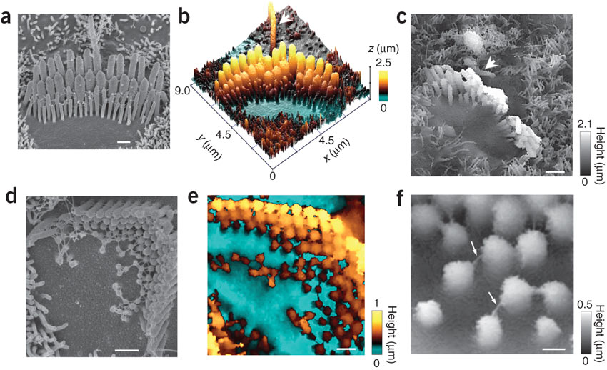
SICM visualization of vertically protruding mechanosensitive stereocilia of auditory hair cells. Image obtained from Novak et al., Nature Methods 6 , 279 (2009) with permission.
The proposed project would entail the design and construction of a SICM that can adapt into our existing inverted fluorescence microscope system. This project is part of our larger overall effort of integrating SICM into our high-speed AFM instrumentation capabilities.
In this project, you will:
-learn how to use advanced scanning probe microscopes
-learn how to work with piezoactuators and low current electronics
-gain experience with mechanical design and instrumentation
-test the performance of your system on biological samples
Contact: Georg Fantner: [email protected]
Design of a high-speed amplifier for large capacitive loads
In atomic force microscopy and other scanning probe microscopy a feedback loop tries to follow the topography of a sample by moving it with a piezoceramic actuator. Nearly all feedback in high-speed scanning probe microscopy is limited by how fast the mechanics can follow the control signals. However, actuators that are able to move sufficiently fast often act as very large capacitances.
While big capacitive loads are difficult to drive at slow speeds, using linear amplifiers becomes almost impossible when going to high speeds as instabilities occur.
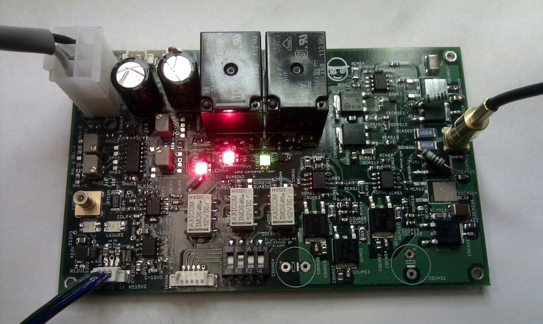
Figure: Prototype of non-linear amplifier.
In this project you will design, build and test a non-linear amplifier circuit capable of driving nearly arbitrary capacitive loads while achieving positioning speeds in the meters per second.
While doing this project you will:
- Get experience in the design of high speed analog circuits with a large current handling capability.
- Learn how to build printed circuit boards with conventional and reflow soldering equipment.
- Get insights into the world of analog electronics beyond normal linear systems.
Contact: Georg Fantner: [email protected]
Fabrication of advanced polymer cantilevers for use in High-Speed Atomic Force Microscopy
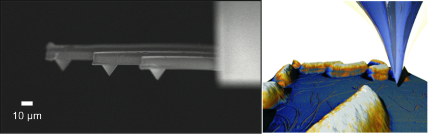
The next frontier in Atomic Force Microscopy (AFM) is to move from single high-resolution images to nanometer resolution video microscopy. Such a technique would have wide applications in areas such as industrial process control in the semiconductor and pharmaceutical industries as well as basic research in polymer-, materials-, and life-sciences. One of the primary limitations towards achieving video-rate AFM is the lack of cantilever probes with sufficient mechanical properties. We have previously created prototype polymer cantilevers that demonstrate improved mechanical properties for a higher imaging bandwidth. In this project, you will create the next generation of polymer cantilevers that will enable operation in the MHz regime.
In this project you will learn:
- design of MEMS structures
- advanced clean room processing techniques,
- mechanical characterization of sub-micron MEMS structures (interferometry, scanning electron microscopy)
- integration into a larger mechatronic system, and
- advanced AFM techniques.
Contact: Georg Fantner: [email protected]
Microfluidic cellular immobilization for improved Atomic Force Microscopy of microbial cells
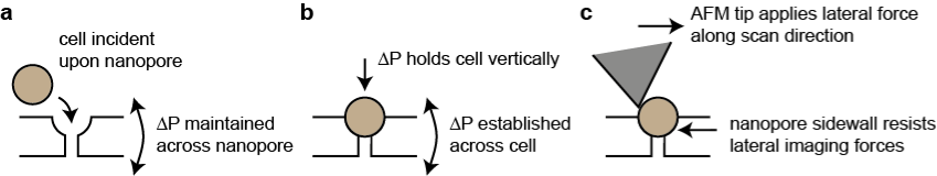
Atomic force microscopy (AFM) is a unique microscopy technique in that it can image and probe biological samples in physiological solutions with nanometre precision. However, for successful imaging the sample must be properly immobilized. This has proven especially difficult for microbial cells and has limited the ability to perform AFM experiments on these cells. The goal of this project is to overcome this limitation by creating advanced microfluidic devices that will immobilize microbial cells in a manner compatible with the AFM.
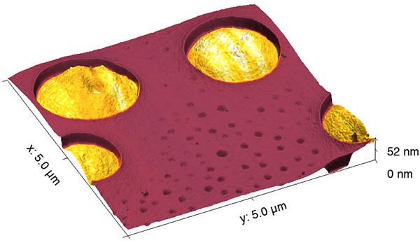
We have designed and fabricated a prototype architecture to trap cells using nanopores coupled to microfluidic channels. The goal of this project is to design the next generation of the nanopore trapping structure.
In this project, you would:
· learn how to design and simulate advanced microfluidic devices
· learn about and apply advanced micro- and nano-fabrication techniques
· learn about bacterial cell culturing and AFM imaging of bacterial cells
· test your device using a combination of AFM imaging and optical microscopy.
Contact: Georg Fantner: [email protected]
Implementation of a modular scan engine for piezo-actuator based scanning probe microscopy with feed-forward compensation
The scan engine is one of the fundamental parts of a scanning probe microscope. The piezoelectric actuators used to move the sample relative to the measurement head are imperfect by nature. A good scan engine that models and compensates unwanted motions like hysteresis or creep is essential to obtain high-quality measurements at the nanoscale. In the scope of a master thesis, such intrinsic errors to the scanning can addittionally be improved live by using digital signal processing and highly precise real-time measurements using MEMS position sensors.
In this project you will:
- Take part in the creation of an open-source high-speed AFM platform.
- Learn to program both backend hardware based on high-end field programmable gate arrays (FPGA) as well as user frontends based on Labview.
- Gain experience into the highly efficient processing of large data streams produced by measurement hardware using digital signal analysis and computer vision.