! Cleanroom humidity warning !
Control of the relative humidity (RH) in photolithography zones is extremely critical. Stable and reproducible photolithography is expected within 38% to 48% RH range.
- In case of low RH (< 38%), the resist sensitivity and development rate decreases. It is then recommended to increase the exposure dose to compensate.
- In case of high RH (> 48%), the resist adhesion decreases. It is then recommended to do an additional bake (>10 minutes @ 150°C) before loading the wafers in the HMDS or coating equipment.
Wafer surface preparation
Usually adhesion of photoresist on inorganic materials is poor resulting in losses of fine structures after development. To solve the issue, silicon wafers are generally treated using the HMDS vapor prime treatment before spincoating the photoresist. Details about the HMDS process and control can be found here: link
Assuming wafers with a clean surface free of organic contamination, the best adhesion will be obtained with the surface preparation recommended in the table:
| Surface material (larger area) | Vapor HMDS | Plasma O2 | Thermal dehydratation |
|---|---|---|---|
| Si | √√ | √ | √ |
| SiO2, fused silica, SiN, Si3N4 | √√ | √ | √ |
| Float glass, pyrex | √ | √√ | √ |
| Metals: Al, Au, Pt, Ti | … | √ | √√ |
| Metals: Ag, Cu, Cr, Fe | … | X | √√ |
| III/V semiconductors (GaN, GaAs) | … | X | √√ |
Legend: √√ Strongly recommended / √ Alternative process / … Not effective / X May affect or destroy underlaying material
Spincoating
The AZ ECI 3007 and ECI 3027 spincurves are shown below, as well as process details for both automatic and manual coating.
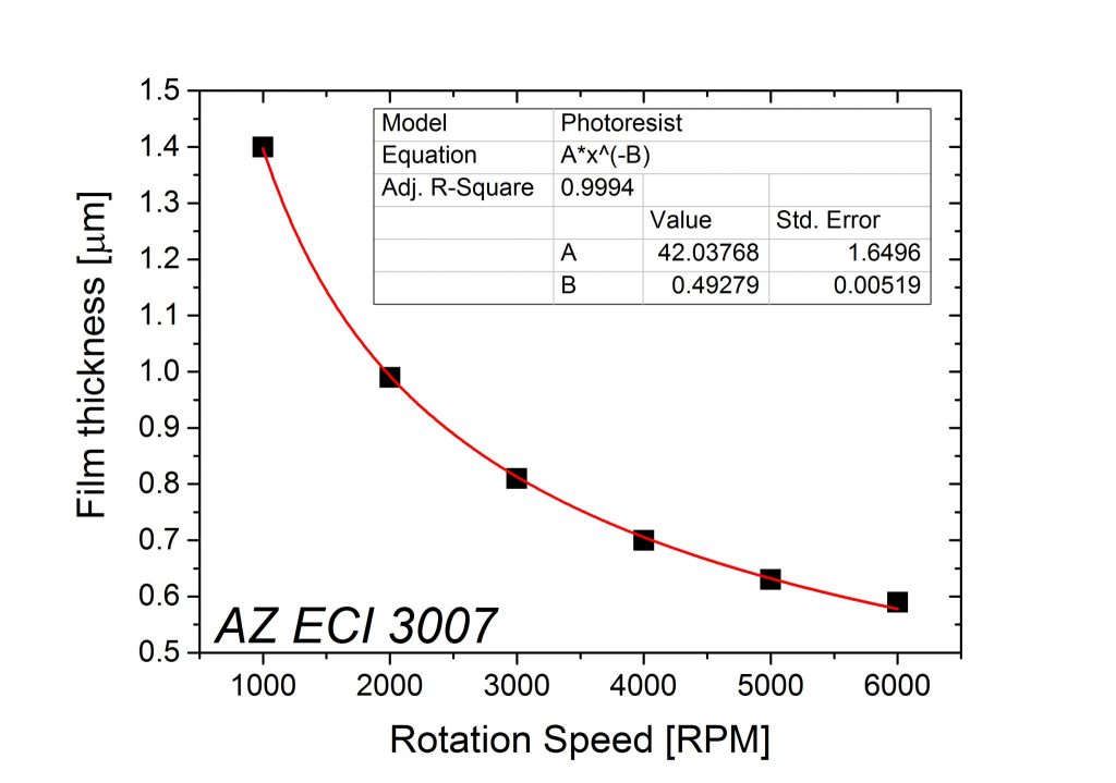
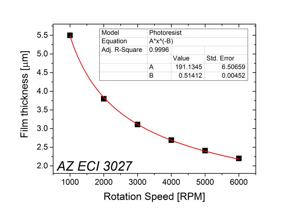
Available thicknesses: 0.6 um / 1 um / 1.5 um / 2.6 um / 4.2 um
Coating:
| PR thickness [μm] | PR | Dispense method | Spin speed [RPM] | Spin duration [sec] | Notes |
|---|---|---|---|---|---|
| 0.6 | ECI 3007 | dynamic, 500RPM | 6000 | 40 | |
| 1 | ECI 3007 | dynamic, 1650RPM | 2050 | 40 | |
| 1.5 | ECI 3007 | dynamic, 850RPM | 850 | 40 | postbake BSR/EBR |
| 2.6 | ECI 3027 | dynamic, 1650RPM | 6000 | 40 | |
| 4.2 | ECI 3027 | dynamic, 1650RPM | 1650 | 40 | postbake BSR/EBR |
Softbake:
| PR thickness [μm] | Bake method | Temperature [°C] | Bake duration [sec] |
|---|---|---|---|
| 0.6 | minimum proximity | 100 | 90 |
| 1 | minimum proximity | 100 | 90 |
| 1.5 | minimum proximity | 100 | 120 |
| 2.6 | minimum proximity | 100 | 120 |
| 4.2 | minimum proximity | 100 | 180 |
Available sequence options:
- HMDS / EC (edge clean)
- Dehydrate / EC
- No treatment / EC
- HMDS / EBR (edge bead removal)
- Dehydrate / EBR
- No treatment / EBR
Available thicknesses: 0.6 um / 1 um / 2.6 um / 4.2 um
Coating:
| PR thickness [μm] | PR | Dispense method | Spin speed [RPM] | Spin duration [sec] | Notes |
|---|---|---|---|---|---|
| 0.65 | ECI 3007 | dynamic, 1500RPM | 6000 | 30 | |
| 1 | ECI 3007 | dynamic, 1500RPM | 2000 | 30 | |
| 2.6 | ECI 3027 | dynamic, 1800RPM | 6550 | 30 | |
| 4.2 | ECI 3027 | dynamic, 1800RPM | 1525 | 30 |
Softbake:
| PR thickness [μm] | Bake method | Temperature [°C] | Bake duration [sec] |
|---|---|---|---|
| 0.6 | proximity – 150um | 90 | 60 |
| 1 | proximity – 150um | 90 | 60 |
| 2.6 | proximity – 150um | 100 | 60 |
| 4.2 | proximity – 150um | 100 | 60 |
Available sequence options:
- HMDS / EC (edge clean)
- Dehydrate / EC
- No treatment / EC
- HMDS / EBR (edge bead removal)
- Dehydrate / EBR
- No treatment / EBR
- Find the spin-coating speed “XXXX” [RPM] matching your target thickness from the AZ ECI 3007 spincurve.
- When coating on wafers, use the STD_”XXXX” recipe, which includes a 500 RPM spreading step and 40 seconds of main coating step.
- When coating on small chips, use the CHIP_”XXXX” recipe, which includes 40 seconds of main coating step and a short acceleration at the end to reduce edge bead effects.
- Softbake temperature: 90°C
- Softbake time: 30” + 30”/um
Exposure
The following table lists the recommend dose “to clear” for the AZ ECI photoresist series coated on silicon wafers. It is recommended to perform a contrast curve / exposure matrix calibration for wafers other than silicon.
| Illumination: | Broadband* | i-line (355-365 nm) | h-line (405 nm) |
|---|---|---|---|
| Equipment: | MA6 Gen3 (no filter) | VPG 200, MA6 Gen3 (filter), MJB4 | MLA 150 |
| PR thickness [µm] | Dose [mJ/cm2]+ | Dose [mJ/cm2]++ | Dose [mJ/cm2]+++ |
| 0.6 | 96 | 100 | Refer to Resist Tables |
| 1 | 115 | 120 | |
| 1.5 | 145 | 150 | |
| 2.6 | 200 | 210 | |
| 4.2 | 330 | 350 |
* Mercury Lamp, Mask Aligner with UV400 configuration & no filter / + Based on intensity readings from Süss optometer broadband CCD / ++ Based on intensity readings from Süss optometer i-line CCD / +++ Based on MLA150 internal dose measurements
Development
The recommended developer for AZ ECI photoresist series is AZ 726 MIF (or MF CD 26), an organic solution based upon TMAH.
IMPORTANT: AZ ECI are chemically amplified resists and requires a post-exposure bake (PEB) before development. On automated development equipment, the PEB is included in the development sequences. For manual development, make sure to perform the PEB as indicated in the section below!
Development sequences for the AZ ECI resist family on the ACS 200 are detailed below:
Post-exposure bake (PEB):
The PEB step is part of the standard development recipes on the ACS 200 system.
| PR thickness [μm] | Bake method | Temperature [°C] | Bake duration [sec] |
|---|---|---|---|
| 0.6 | minimum proximity | 110 | 60 |
| 1 | minimum proximity | 110 | 60 |
| 1.5 | minimum proximity | 110 | 60 |
| 2.6 | minimum proximity | 110 | 90 |
| 4.2 | minimum proximity | 110 | 90 |
Development:
| PR thickness [μm] | Developer | Dev. method | Cycle time [sec] | N° of cycles |
|---|---|---|---|---|
| 0.6 | AZ 726 MIF | puddle | 30 | 2 |
| 1 | AZ 726 MIF | puddle | 30 | 2 |
| 1.5 | AZ 726 MIF | puddle | 30 | 2 |
| 2.6 | AZ 726 MIF | puddle | 30 | 2 |
| 4.2 | AZ 726 MIF | puddle | 30 | 3 |
In case of non-complete PR dissolution with the standard development duration, please use any of the D4+(X)-726MIF sequences to add some development time.
Development sequences for the AZ ECI resist family on the EVG 150 are detailed below:
Post-exposure bake (PEB):
The PEB step is part of the standard development recipes on the EVG 150 system.
| PR thickness [μm] | Bake method | Temperature [°C] | Bake duration [sec] |
|---|---|---|---|
| 0.6 | proximity – 300um | 110 | 90 |
| 1 | proximity – 300um | 110 | 90 |
| 2.6 | proximity – 300um | 110 | 90 |
| 4.2 | proximity – 300um | 110 | 90 |
Development:
| PR thickness [μm] | Developer | Dev. method | Cycle time [sec] | N° of cycles |
|---|---|---|---|---|
| 0.6 | AZ 726 MIF | puddle | 50 | 1 |
| 1 | AZ 726 MIF | puddle | 50 | 1 |
| 2.6 | AZ 726 MIF | puddle | 50 | 1 |
| 4.2 | AZ 726 MIF | puddle | 50 | 1 |
In case of non-complete PR dissolution with the standard development duration, please use any of the D4+(X)-726MIF sequences to add some development time.
- PEB temperature: 100°C
- PEB time: 60” (ECI 3007) or 90” (ECI 3027)
- Recommended developer: AZ 726 MIF (no dilution needed)
- Development time: 20″-30″/um
- Rinse: H2O 1min
IMPORTANT:
After development, it is mandatory for wafers to go through an additional rinsing step with DI water to avoid backside contamination and damage on equipments (chuck in etcher) in further processing steps. The water baths of the following wet benches can be used free of charge (5 min. billing delay after login):
- Z01 – Plade “Solvent” wet bench
- Z02 – UFT “Resist” wet bench
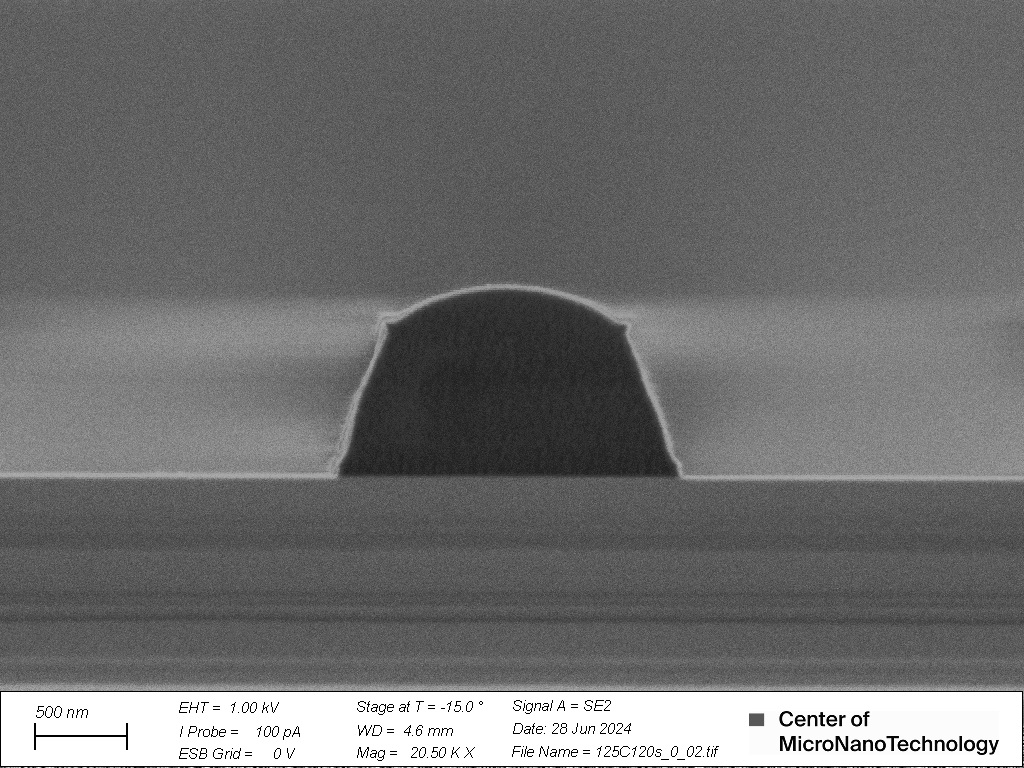
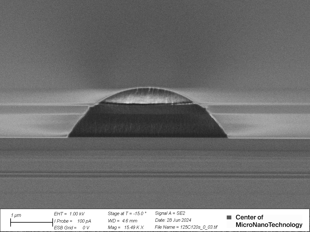
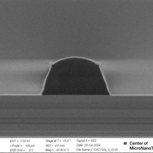
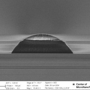
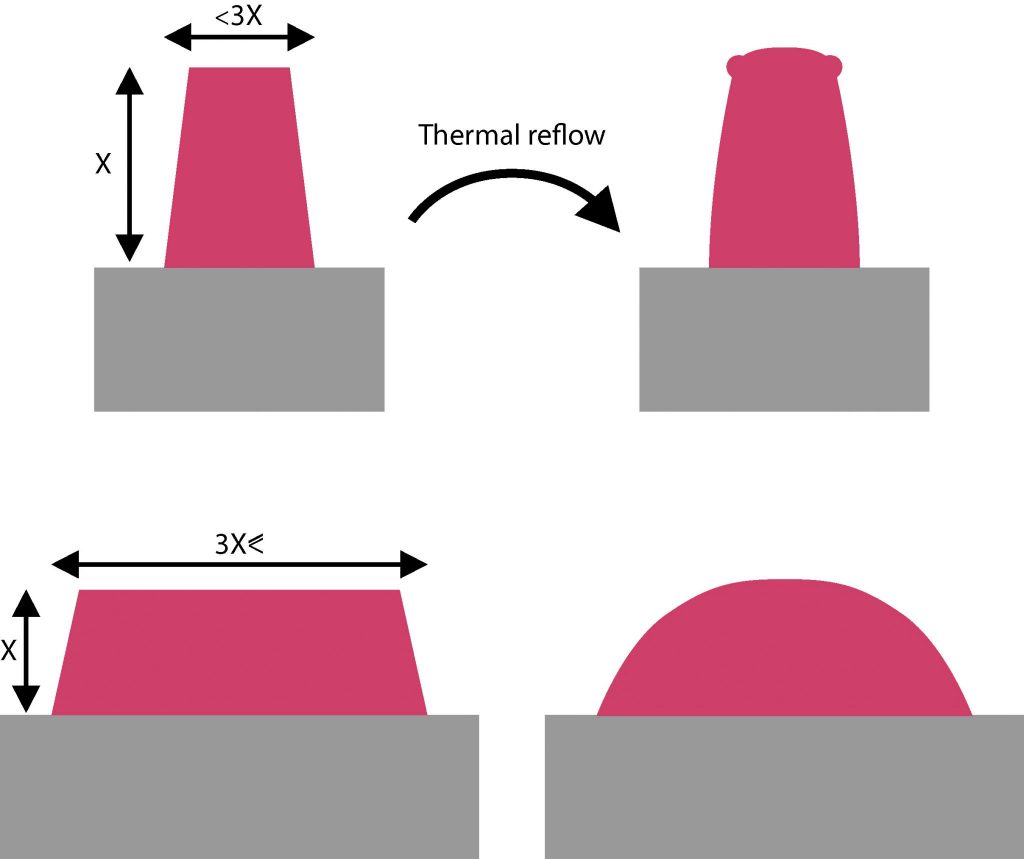
AZ ECI 3007 thermal reflow
Thermal reflow of photoresist is used to smooth and reshape photoresist patterns by heating them above their glass transition temperature. This technique allows the photoresist to flow, reducing surface roughness and achieving more rounded features (important for IBE). It is commonly applied to enhance the profile of microstructures, particularly in applications requiring curved or sloped sidewalls. The reflow process must be carefully controlled to avoid excessive deformation or pattern collapse.
The ratio between height and width of the feature to reflow has a great impact on the result. A threshold is found to be at 1:3 to round the structure / lower the sidewalls slope as presented in the image below.
In practice for AZ ECI 3007:
- Reflow on a hot plate : 120s @ 125°C
- Reflow in ACS200 : 180s or 300s @ 145°C
Time can be adjusted based on the slope desired. Pictures of the results can be seen in the gallery below.
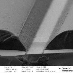
Pictures Gallery