! Cleanroom humidity warning !
Control of the relative humidity (RH) in photolithography zones is extremely critical. Stable and reproducible photolithography is expected within 38% to 48% RH range.
- In case of low RH (< 38%), the resist sensitivity and development rate decreases. It is then recommended to increase the exposure dose.
- In case of high RH (> 48%), the resist adhesion decreases. It is then recommended to do an additional bake (>10 minutes @ 150°C) before loading the wafers in the HMDS or coating equipment.
Wafer surface preparation
Usually adhesion of photoresist on inorganic materials is poor resulting in losses of fine structures after development. To solve the issue, silicon wafers are generally treated using the HMDS vapor prime treatment before spincoating the photoresist. Details about the HMDS process and control can be found here: link
Assuming wafers with a clean surface free of organic contamination, the best adhesion will be obtained with the surface preparation recommended in the table:
| Surface material (larger area) | Vapor HMDS | Plasma O2 | Thermal dehydratation |
|---|---|---|---|
| Si | √√ | √ | √ |
| SiO2, fused silica, SiN, Si3N4 | √√ | √ | √ |
| Float glass, pyrex | √ | √√ | √ |
| Metals: Al, Au, Pt, Ti | … | √ | √√ |
| Metals: Ag, Cu, Cr, Fe | … | X | √√ |
| III/V semiconductors (GaN, GaAs) | … | X | √√ |
Legend: √√ Strongly recommended / √ Alternative process / … Not effective / X May affect or destroy underlaying material
Spincoating
The AZ 15nXT spincurve is shown below, as well as process details for both automatic and manual coating.
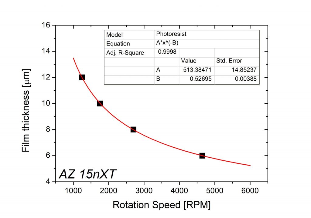
Available thicknesses: 6 um / 8 um / 10 um
Coating:
| PR thickness [μm] | PR | Dispense method | Spin speed [RPM] | Spin duration [sec] | Notes |
|---|---|---|---|---|---|
| 6 | 15nXT | spiral | 4650 | 20 | |
| 8 | 15nXT | spiral | 2690 | 20 | |
| 10 | 15nXT | spiral | 1760 | 20 |
Softbake:
| PR thickness [μm] | Bake method | Temperature [°C] | Bake duration [sec] |
|---|---|---|---|
| 6 | proximity with 60sec ramp | 120 | 120 |
| 8 | proximity with 60sec ramp | 120 | 120 |
| 10 | proximity with 60sec ramp | 120 | 120 |
Available options:
- HMDS / EC (edge clean)
- Dehydrate / EC
- HMDS / EBR (edge bead removal)
- Dehydrate / EBR
- Find the spin-coating speed “XXXX” [RPM] matching your target thickness from the AZ 15nXT spincurve.
- When coating on wafers, use the HV_”XXXX” recipe, which includes a 500 RPM spreading step and 100 seconds of main coating step.
- When coating on small chips, use the CHIP_”XXXX” recipe, which includes 40 seconds of main coating step and a short acceleration at the end to reduce edge bead effects.
- Softbake temperature: 120°C
- Softbake time: 3 minutes
Exposure
The following table lists the typical exposure doses for AZ 15nXT coated on silicon wafers.
Take note that your optimal dose depends on the layout type (isolated, dense lines & spaces, trenches, pillars, holes, etc…) and critical dimension (CD), as well as the wafer surface reflectivity. Please perform a dose series to determine the perfect match between the resulting pattern and the initial CAD layout dimensions.
| Illumination: | i-line (375 nm) | i-line (355-365 nm) |
|---|---|---|
| Equipment: | MLA 150 | MA6 Gen3 (filter) |
| PR thickness [µm] | Dose [mJ/cm2]+ | Dose [mJ/cm2]++ |
| 6 | 210 | >240 |
| 8 | 255 | |
| 10 | 330 |
+ Based on MLA150 internal dose measurements / ++ Based on intensity readings from Süss optometer i-line CCD
Development
The recommended developer for AZ 15 nXT is AZ 726 MIF (or MF CD 26), an organic solution based upon TMAH.
IMPORTANT: AZ 15nXT is a negative resist and requires a post-exposure bake (PEB) before development. On automated development equipment, the PEB is included in the development sequences. For manual development, make sure to perform the PEB as indicated in the section below!
Development sequences for AZ 15nXT are listed below:
Post-exposure bake (PEB):
The PEB step is part of the standard development recipes on the ACS 200 system.
| PR thickness [μm] | Bake method | Temperature [°C] | Bake duration [sec] |
|---|---|---|---|
| 6 | proximity with 20sec ramp | 123 | 100 |
| 8 | proximity with 20sec ramp | 123 | 100 |
| 10 | proximity with 20sec ramp | 123 | 100 |
Development:
| PR thickness [μm] | Developer | Dev. method | Cycle time [sec] | N° of cycles |
|---|---|---|---|---|
| 6 | AZ 726 MIF | puddle | 30 | 3 |
| 8 | AZ 726 MIF | puddle | 30 | 4 |
| 10 | AZ 726 MIF | puddle | 30 | 5 |
In case of non-complete PR dissolution with the standard development duration, please use any of the D4+(X)-726MIF sequences to add some development time.
- ! Important! Make sure to perform the PEB at 120°C for 60 seconds before development.
- Recommended developer: AZ 726 MIF
- Development time: 10″/1um
- Rinse: H2O 1min
IMPORTANT:
After development, it is mandatory for wafers to go through an additional rinsing step with DI water to avoid backside contamination and damage on equipments (chuck in etcher) in further processing steps. The water baths of the following wet benches can be used free of charge (5 min. billing delay after login):
- Z01 – Plade “Solvent” wet bench
- Z02 – UFT “Resist” wet bench