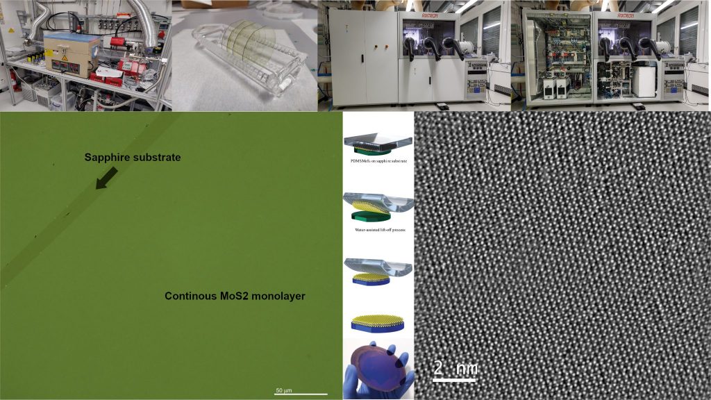
In collaboration with LANES we develop solutions for large-area, wafer-scale growth of electronics-grade 2D semiconductors such as MoS2 and related transition metal dichalcogenides (TMDCs). The unique combination of atomic-scale thickness, direct bandgap, favorable electronic and mechanical properties make this class of materials interesting for applications in high-end electronics, flexible electronics, optoelectronics, spintronics, biosensing, NEMS and MEMS devices etc.
Our platforms are based on in-house developed MOCVD growth system optimized for 3” wafer substrates and commercial system BM Novo system for the growth on 4” wafer substrates. We develop fabrication protocols for transfer and integration in nanofluidics, and optoelectronic devices.
- Thakur M., Macha M., Chenev A, Graf M., Lihter M., Deen J., Tripathi M.M., Kis A. Radenovic A. Wafer-scale fabrication of MoS2 nanopore devices for Single-Molecule Biosensing Small methods , 2000072 DOI: 10.1002/smtd.202000072
- Cun H., Macha M., Kim H.K., Liu K., Zhao Y., Lagrange T., Kis A., and Radenovic A. Wafer-scale MOCVD growth of monolayer MoS2 on sapphire and SiO2, Nano Research 2019; DOI:10.1007/s12274-019-2502-9.
- Cun, H.Y., A. Hemmi, E. Miniussi, C. Bernard, B. Probst, K. Liu, D.T.L. Alexander, A. Kleibert, G. Mette, M. Weinl, M. Schreck, J. Osterwalder, Radenovic, A, and T. Greber, Centimeter-Sized Single-Orientation Monolayer Hexagonal Boron Nitride With or Without Nanovoids, Nano Letters. 2018 18, pp1205-1212.