Abstract
This document outlines the research activities of the Mobile Communications Lab of the Swiss Federal Institute of Technology (EPFL Lausanne) in the area of Software Radio architectures. A radio test bed being developed for providing real-time wideband radio communication capabilities in a form attractive for university research and teaching is described. It will be used to implement signaling methods similar, but not limited to, evolving 3rd generation radio standards (e.g. UMTS, CDMA2000).
Keywords
Software Radio, 3rd Generation Mobile Communication Systems, University Research and Teaching
Introduction
The purpose of this document is to provide an outline of a Real-Time Software Radio platform currently being developed at EPFL’s Mobile Communication Laboratory (LCM) for the purpose of university research and teaching. Various aspects of this project are being carried out with our partners, Institut Eurécom (Sophia Antipolis, France), Nokia and STMicroelectronics (Geneva, Switzerland).
The research activities of the LCM are primarily motivated by our interests in communication theory, and its application to real-world problems. Despite the fundamental nature of our focus, we are investing a considerable effort in the development of a real-time “software”radio testbed. Although there is a substantial hardware component, its function is essentially to create a window in the frequency range of interest, take its content and move it to a more convenient frequency interval where it is sampled directly. The samples are then passed directly to the memory of a PC.
All signal generation and processing (e.g. multiple-access, power control, coding, IF filtering) are completely software defined. This type of architecture is particularly appealing for a university research and teaching program, since the minimal hardware component permits “user-friendly” testing of advanced signaling techniques.
The testbed’s characteristics (e.g. frequency bands, bandwidth, transmit power, receiver sensitivity, multiple users) are comparable to those of the evolving 3rd generation radio standards http://www.bakom.ch (e.g. MTS,IMT-2000, ITT DoKoMo). We are, however, by no means limited to the restrictions imposed by these standards.
One aspect where our testbed diverges from the evolving standards is that it will be based on time-division duplex. We believe this to be more interesting for research in such areas as dynamic resource allocation and multi-antenna processing since we can take advantage of channel reciprocity at the transmitter.
The design is flexible enough to allow for real-time emulation of both a powerful multi-antenna basestation and advanced terminals.
We are committed to examining implementation aspects of advanced signaling/reception techniques such as
-
Multiuser receivers (stripping, interference cancellation) 2)
-
Wideband channel estimation and synchronization
Portions of this testbed will be used in the classroom, in order to expose students to implementation issues which surface in real-time signal processing. This will complement theoretical courses in modern digital communications and give students a global vision of communication systems. It is our hope that this testbed will also stimulate interest in advanced radio design techniques, by opening up many avenues for student projects, both at the undergraduate and graduate level.
Hardware Overview
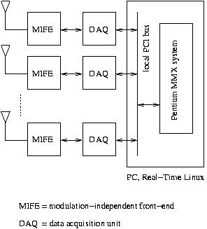
The figure below shows an overview of the hardware components in its most complex arrangement (i.e. a multi-antenna basestation)
Each antenna is connected to a modulation-independent front-end (MIFE) which implements a two-way mapping between transmit/receive samples and transmit/receive radio frequency waveforms. An intelligent PCI-based data-acquisition unit (DAQ) is responsible for transferring the samples between the MIFEs and the memory inside the PC. Although state-of-the-art components are used, the hardware portion is kept to a strict minimum and is both extremely flexible and digitally controllable.
-
Modulation-Independent Front-End (MIFE)
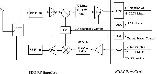
The figure below shows a simplified block diagram of our MIFE.
On reception (Rx), the RF signal is filtered, amplified and down-converted to a 70MHz intermediate frequency (IF).
The local oscillator frequency is digitally tunable in steps of a few kHz. This is amplified by a digitally tunable gain control and directly sampled at around 15 MSamp/s. The samples are transfered via a ribbon cable using high-speed line drivers to the DAQ.
On the transmission end (Tx), samples from the DAQ arrive at a rate of around 15 MSamp/s and drive a hardware up-sampling circuit and a high-speed D/A converter (around 120 MSamp/s) to directly synthesize the 70MHz IF signal. This signal is then amplified, up-converted to RF, filtered and amplified by a variable-gain power amplifier.
Special low-speed control lines control the gains of the Rx AGC and Tx Power Amp, LO frequency, as well as the antenna switch. Although not included in the figure, automatic wide-band calibration capabilities (for both Tx and Rx) are included in the design, which are required for multi-antenna systems.
The basic characteristics of the MIFE are summarized in this table:
| MIFE Charateristics | |
|---|---|
| Frequency Bands | 2100-2170 MHz, 1885-2025 MHz |
| Bandwidth | 5 MHz (initially) |
| Transmit Power (per antenna) | 1 W |
| Receiver Sensitivity | -120 dBm |
| Noise Figure | < 5 dB |
| Input IP3 | > -7 dBm |
| Duplex mode | Time Division (TDD) |
| Rx Gain Control | digital tuning, 1dB steps over 40dB |
| Tx Power Control | digital tuning, 1dB steps over 80dB |
| Local Oscillator | digital control, Tx and Rx |
| RF Calibration | digital control |
| Direct IF sampling (70 MHz) on Rx | 12-bit A/D @ 14.7456 MSamp/s |
| Direct IF synthesis (70 MHz) on Tx | 12-bit D/A @ 117.9648 MSamp/s |
| Digital Interface | High speed: Low-Voltage Differential Signaling (LVDS) Low speed: 3.3V HCMOS line drivers |
The MIFE is actually composed of three Eurocard format PCBs. Click here to see pictures
-
Data Acquisition Unit
The data acquisition unit is a PCI bus-mastering device permitting high-speed full duplex parallel transfer of digital data from an external device. We have opted for a PCI architecture since it is the most general purpose bus architecture and is used on most standard PCs, as well as DSP systems. It consists of two components, namely a powerful Xilinx Field Programmable Gate Array (FPGA) XCV300 and a bus-mastering PCI controller PLX9080. The design is based on a modification of the SBX+ reconfigurable interface architecture available in the public domain. The format was changed from a standard PCI card to a PCI Mezzanine Card (PMC) to allow for integration into embedded DSP architectures and ordinary PCs.
Intelligent firmware on the FPGA for transferring data via the DMA engines of the PLX9080 to the host (DSP, CPU) memory has been developed. After an initial configuration phase, transfers are continuous and completely transparent to the host, which just “sees” a circular buffer containing samples acquired/to be transfered from/to the external MIFE.
The basic components which make up the DAQ are the following
-
Line Drivers/Receivers for transfer from external devices via ribbon-cables
-
Reconfigurable FPGA-based 16-bit bi-directional interface external device (up to 30 Msamp/s full-duplex)
-
PCI bus-mastering controller for direct transfer of samples to/from memory (DMA) on PCI-based signal processing units (e.g. DSP cards (C6x, StarCore, Sharc)), workstations (Pentium MMX, SPARC VIS, PowerPC AltiVec, Alpha), embedded processor cards, etc.)
-
Processor Mezzanine Card (PMC) form-factor for maximum flexibility