! Cleanroom humidity warning !
Control of the relative humidity (RH) in photolithography zones is extremely critical. Stable and reproducible photolithography is expected within 38% to 48% RH range.
- In case of low RH (< 38%), the resist sensitivity and development rate decreases. It is then recommended to increase the exposure dose.
- In case of high RH (> 48%), the resist adhesion decreases. It is then recommended to do an additional bake (>10 minutes @ 150°C) before loading the wafers in the HMDS or coating equipment.
Perforated Carrier Wafer Layouts
In order to rapidly and efficiently release wafers, temporary bonded with WaferBOND HT-10.11, with a solvent-based chemical method, it is strongly recommended to have one of the two wafers (device or carrier) that includes through silicon vias (TSV):
- On the device wafer, this can typically be achieved at the last step of the process by including a DRIE or partial dicing step up to the WaferBOND layer to have singled out chips ready for release.
- On the handle wafer, perforations with specific layouts can be used, that are compatible with handling in automatic coater/developer equipment. Such carrier wafers are fabricated by DRIE / grinding / CMP.
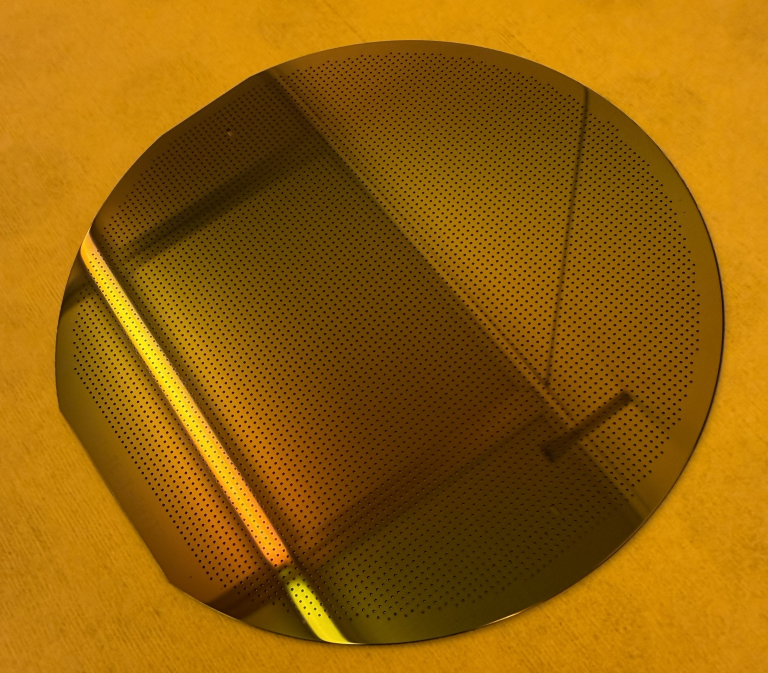
Layouts with two different hole densities & diameters are available to download below:
Wafer surface preparation
In order to obtain maximum process reliability and bonding performances, wafers should be cleaned beforehand, to remove organic and particle contaminations:
- Silicon wafers: RCA cleaning in Plade RCA (staff service)
- Glass wafers: Piranha cleaning in UFT Piranha
Prior to the application of WaferBOND, optimal adhesion will be obtained with the surface preparation recommended in the table:
| Surface material (larger area) | Vapor HMDS | Plasma O2 | Thermal dehydratation |
|---|---|---|---|
| Si | … | √√ | √√ |
| SiO2, fused silica, SiN, Si3N4 | … | √√ | √√ |
| Float glass, pyrex | … | √√ | √√ |
| Metals: Al, Au, Pt, Ti | … | √ | √√ |
| Metals: Ag, Cu, Cr, Fe | … | X | √√ |
| III/V semiconductors (GaN, GaAs) | … | X | √√ |
Legend: √√ Strongly recommended / √ Alternative process / … Not effective / X May affect or destroy underlaying material
Spincoating
Waferbond is applied by spin-coating on only one wafer, the non-perforated one.
The WaferBOND HT-10.11 spincurve is shown below, as well as process details on the Sawatec “MISC” manual coater.
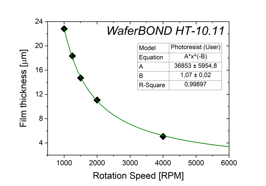
- Find the spin-coating speed “XXXX” [RPM] matching your target thickness from the WaferBOND HT-10.11 spincurve. In general, we recommend to target a thickness that allows to compensate for the wafers TTV.
- When coating on wafers, use the “WBOND-CMI” recipe, which consists in 30 seconds of main coating step, with an acceleration of 500 RPM/s. Spinning at 1200 RPM results in a ~20um film.
- Softbake (Use both hotplates!):
- Step N°1: 120°C, 3 minutes
- Step N°2: 180°C, 4 minutes
Cleaning of backside contaminations
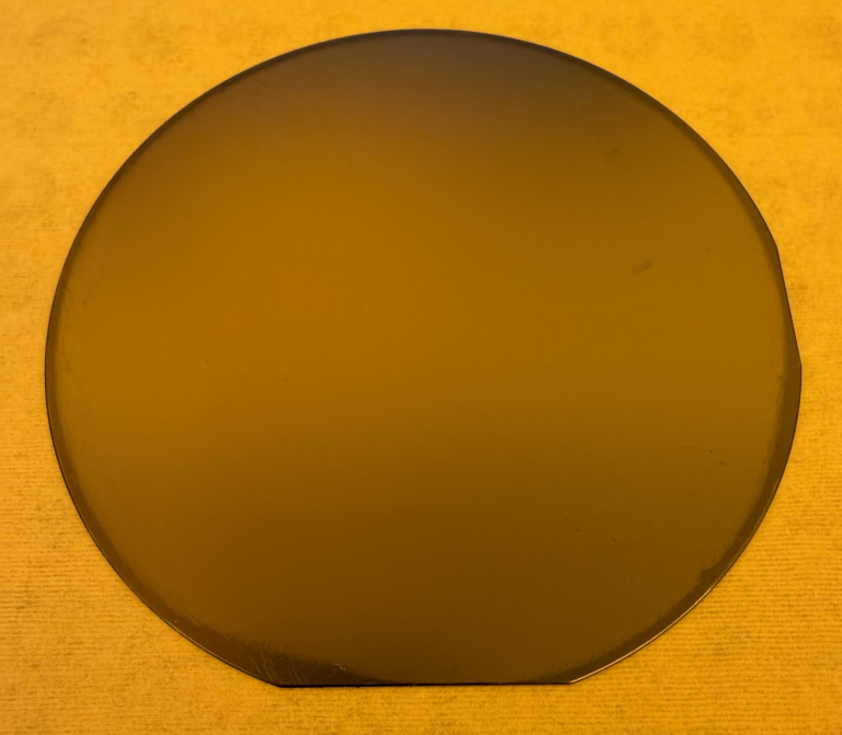
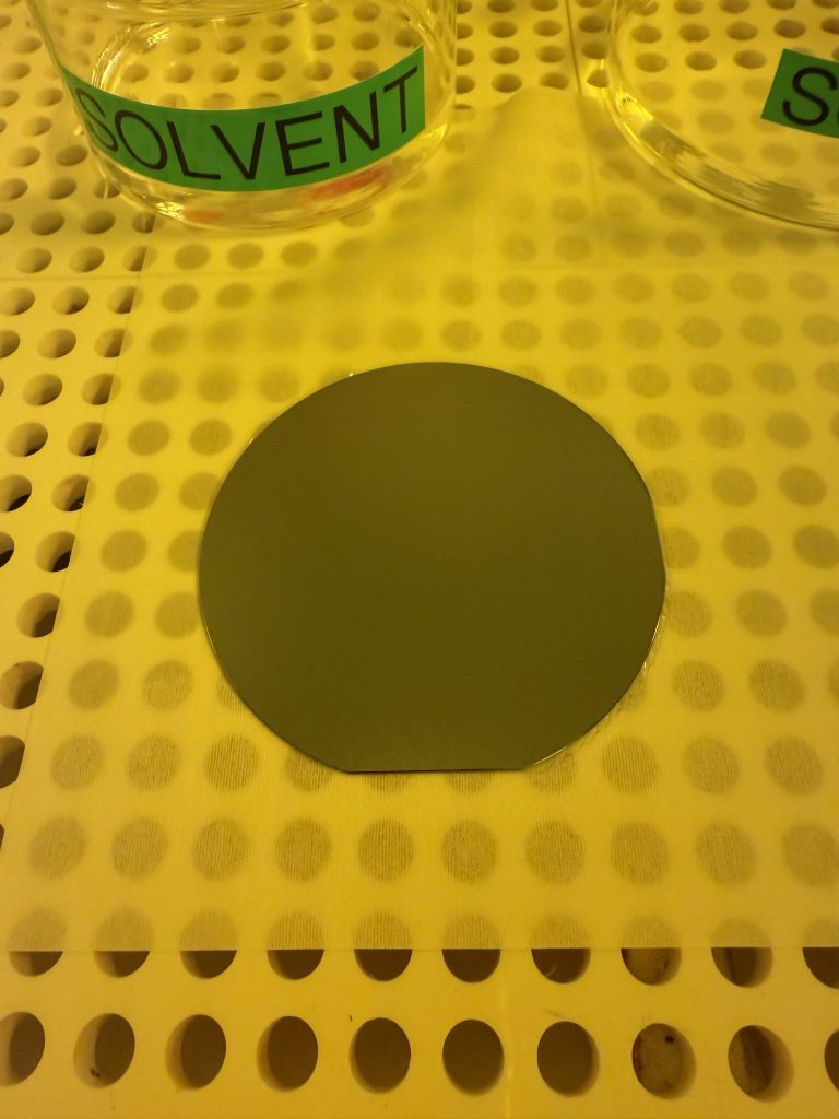
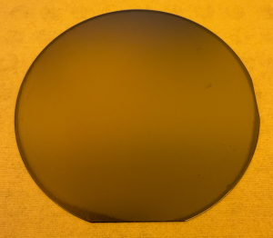
After coating, the edges of the wafer backside will be contaminated with spiderweb-like polymer residues. This contamination needs to be cleaned before loading the wafers on the EVG 510 bond chuck
The process involves:
- Protecting the WaferBOND coating side with UV tape in Zone 11. Details on the application and removal of the UV tape can be found here: https://www.epfl.ch/research/facilities/cmi/wp-content/uploads/2020/03/POWATEC.pdf
- Cleaning on the Arias Solvent bench in Zone 13:
- Immerging the wafer in WaferBOND Remover for ~ 5 minutes at room temperature.
- Rinsing in IPA for ~ 1 minute.
- Dry with N2 gun.
Wafer bonding
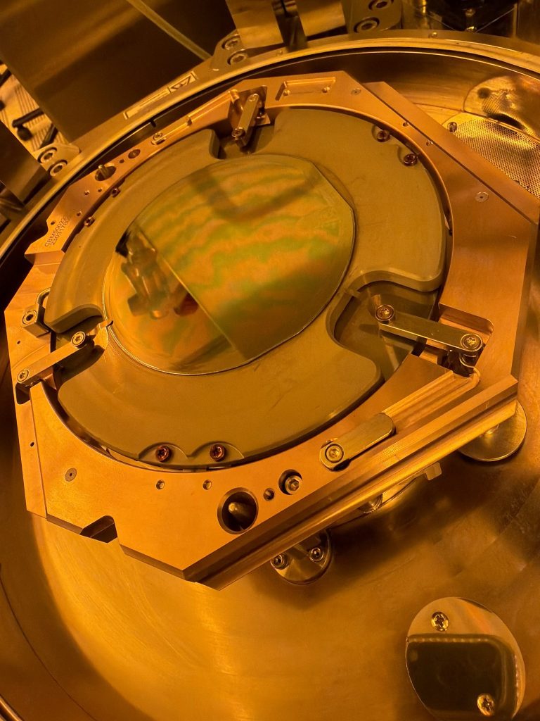
Here is a summary of the bonding sequence steps, implemented in the EVG 510 wafer bonder, to bond 4inch wafers, with an intermediate 20um WaferBOND layer:
- Ramp the pressure plates temperature to 180˚C (ramp 20°C/min)
- Establish vacuum and wait until P < 5 mbar (low vacuum)
- Ramp the piston force and hold at 0.9 kN (0.58 MPa) for 2 minutes
- Release the piston force
- Cooldown
- Release vacuum
- Remove bonded wafers
| Wafer Size | Waferbond Thickness | Temperature | Force |
|---|---|---|---|
| [inch] | [µm] | [°C] / [sec] | [kN] |
| 4 | 20 | 180 / 120 | 0.9 |
Sample debonding & release
After processing the device wafer, the samples will be separated using WaferBOND Remover on the Arias solvent wet bench of Zone 13. Depending on the layout of the perforations, the process can take quite a long time and heating of WaferBOND remover beaker is recommended to speed up the process.
The process consists in:
- Immersion in heated (80°C) WaferBOND Remover, duration: 2-4 hours or until separation. Use the bain-marie integrated in the bench. PLEASE LABEL !
- Immersion (rinsing) in RT WaferBOND Remover, duration: >30 minutes
- Rinsing in IPA for ~ 1 minute.
- Dry with N2 gun.