! Cleanroom humidity warning !
Control of the relative humidity (RH) in photolithography zones is extremely critical. Stable and reproducible photolithography is expected within 38% to 48% RH range.
- In case of low RH (< 38%), the resist sensitivity and development rate decreases. It is then recommended to increase the exposure dose.
- In case of high RH (> 48%), the resist adhesion decreases. It is then recommended to do an additional bake (>10 minutes @ 150°C) before loading the wafers in the HMDS or coating equipment.
Wafer surface preparation
In order to obtain maximum process reliability and bonding performances, wafers should be cleaned beforehand, to remove organic and particle contaminations:
- Silicon wafers: RCA cleaning in Plade RCA (staff service)
- Glass wafers: Piranha cleaning in UFT Piranha
Prior to the application of PermiNEX polymers, optimal adhesion will be obtained with the surface preparation recommended in the table:
| Surface material (larger area) | Vapor HMDS | Plasma O2 | Thermal dehydratation |
|---|---|---|---|
| Si | … | √√ | √√ |
| SiO2, fused silica, SiN, Si3N4 | … | √√ | √√ |
| Float glass, pyrex | … | √√ | √√ |
| Metals: Al, Au, Pt, Ti | … | √ | √√ |
| Metals: Ag, Cu, Cr, Fe | … | X | √√ |
| III/V semiconductors (GaN, GaAs) | … | X | √√ |
Legend: √√ Strongly recommended / √ Alternative process / … Not effective / X May affect or destroy underlaying material
Spincoating
The Perminex 1005 & 2005 spincurves are shown below, as well as process details on the Sawatec “MISC” manual coater. Other Perminex grades can be used on the Sawatec “MISC” by following the recommendations from the supplier’s technical datasheet.
Note: The Perminex 2000 serie doses are stored at -15°C to preserve their lifetime. Make sure to take a dose out of the freezer at least 1 hour before use in order to let it warm up to room temperature. Put it back in the freezer after use.
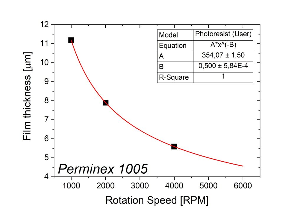
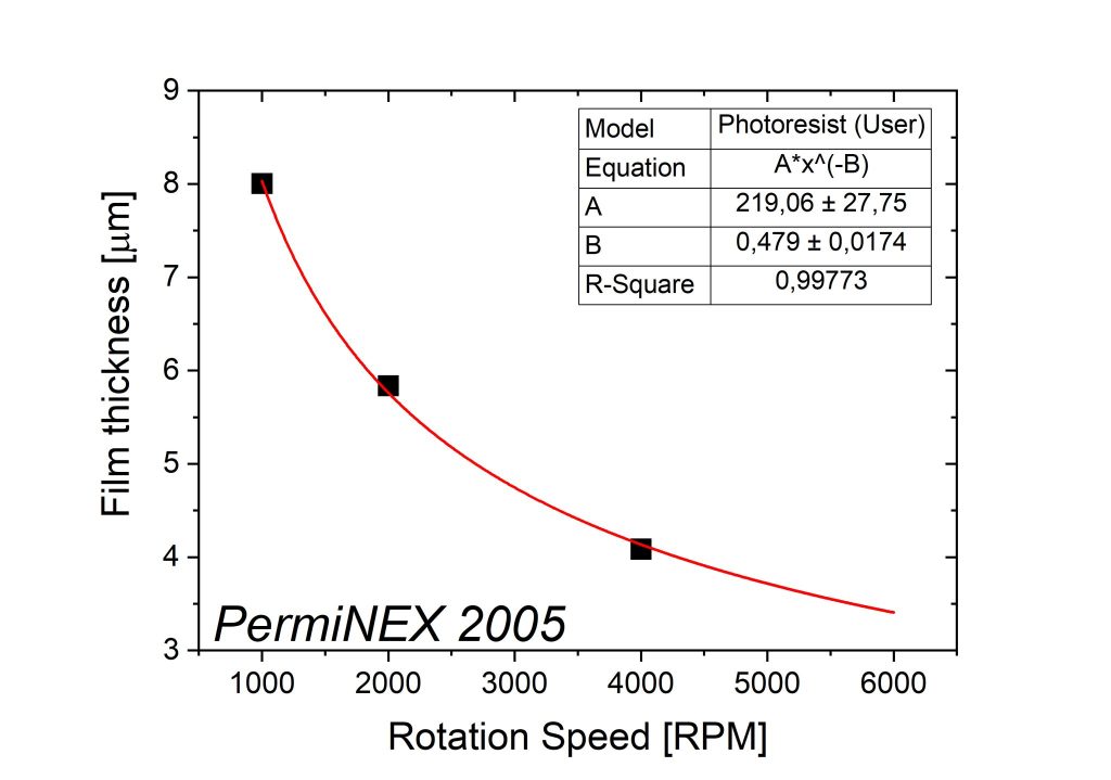
- Find the spin-coating speed “XXXX” [RPM] matching your target thickness from the Perminex spincurves. In general, we recommend to target a thickness that allows to compensate for the wafers TTV.
- When coating on wafers, use the “PNEX2005” recipe, which includes a 5 seconds 500 RPM spreading step and 30 seconds of main coating step.
- Perminex 1005: Spinning at 1000 RPM results in a 11um thick film.
- Perminex 2005: Spinning at 1000 RPM results in a 8um thick film.
- Softbake temperature: 95°C
- Softbake time:
- Perminex 1005 – 11um: 10 minutes
- Perminex 2005 – 8um: 8 minutes
Edge Bead Removal
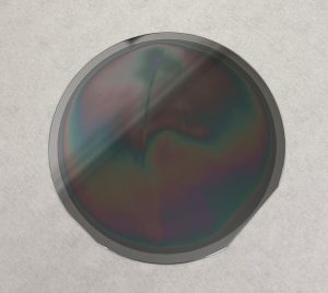
An edge bead removal step is recommended to obtain optimal exposure quality on the Süss MA6 gen3 mask-aligner, and to avoid contamination from the Perminex polymer on the bond chuck of the EVG 510.
The edge bead removal is done using the EBR PG solvent of the EVG 150 automated coater. Programs are available in the “Miscellanous” category to perform EBR for 3mm or 5mm from the wafer edge, and 60 seconds duration.
Exposure
The following table lists some exposure doses for Perminex 1005 & 2005 coated on silicon wafers.
Perminex should be exposed on a mask-aligner (MA6 Gen3) with 365nm i-line illumination. While Perminex can potentially be exposed with the 375nm laser of the MLA 150, the very high dose requirements significantly limit its practical use since a 4 inch wafer will require > 4 hours of exposure.
| Illumination: | i-line (365 nm) | i-line (375 nm) | |
|---|---|---|---|
| Equipment: | MA6 Gen3 (filter) | MLA 150 | |
| Resist grade | PR thickness [µm] | Dose [mJ/cm2]++ | Dose [mJ/cm2]+ |
| Perminex 1005 | 11 | ~720 | >7200 |
| Perminex 2005 | 8 | ~1200 | > 12000 |
+ Based on MLA150 internal dose measurements / ++ Based on intensity readings from Süss optometer i-line CCD
Development
The recommended developer for the Perminex 2000 serie is AZ 726 MIF (or MF CD 26), an aqueous organic solution based upon TMAH, while The Perminex 1000 serie uses PN 1000, a propriety solvent blend developer.
IMPORTANT: Perminex is a negative-tone resist and requires a post-exposure bake (PEB) before development. For manual development, make sure to perform the PEB as indicated in the section below!
Observations: After development, the resist profile will be slightly negative (especially when exposed @ 365nm) and some resist footing (contamination at the surface/resist interface) might be difficult to develop & clear properly.
- ! Important! Make sure to perform the PEB at 70°C for 120 seconds before development.
- Recommended developer: PN 1000
- Development time (11 um thick film): 8′ (beaker N°1) + 20” (beaker N°2)
- Dry: N2 blow
- ! Important! Make sure to perform the PEB at 70°C for 120 seconds before development.
- Recommended developer: AZ 726 MIF
- Development time (8 um thick film): 1’15” (beaker N°1) + 15” (beaker N°2)
- Rinse: H2O > 30sec
- Dry: N2 blow
Post-development bake & Descum
After development, two additional steps are recommended before trying to bond:
- Post-development bake: 180°C for 5 minutes to dry & eliminate the residual developer content from Perminex the film.
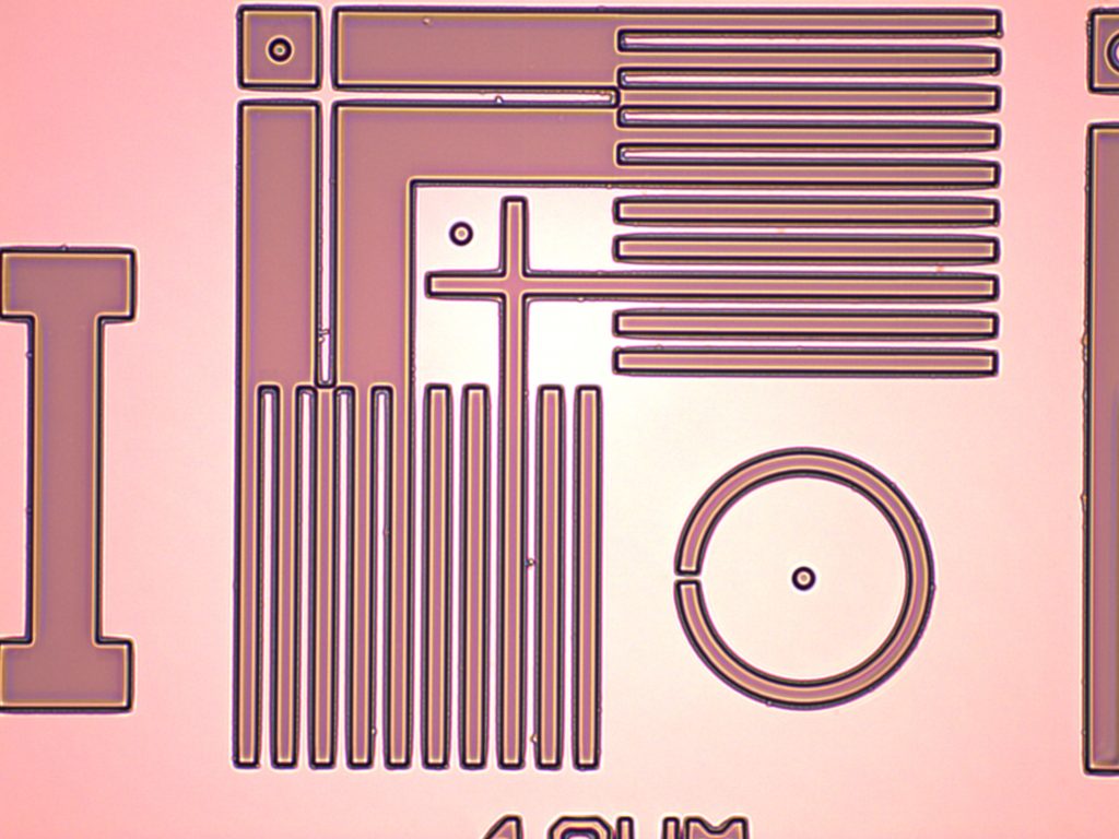
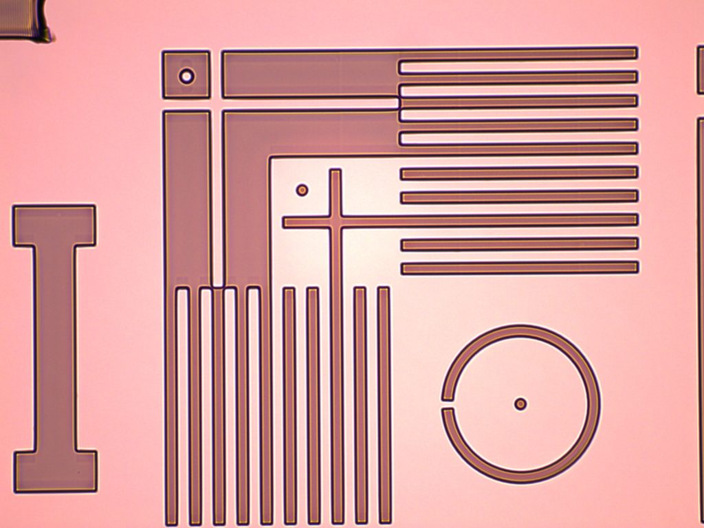
- Descum: A short plasma O2 descum (power < 100W, time < 20sec) will allow to clear resist footing contamination especially from high aspect ratio structures (see images below). A slight thickness loss is expected after descum.
Wafer bonding
Here is a summary of the bonding sequence steps, implemented in the EVG 510 wafer bonder, to bond 4inch wafers:
- Ramp the pressure plates temperature to 150˚C (ramp 20°C/min)
- Establish vacuum and wait until P < 0.5 mbar (low vacuum)
- Ramp the piston force and hold at 5 kN (0.58 MPa) for 30 seconds
- Release the piston force
- Ramp the pressure plates temperature to 180˚C (ramp 5°C/min)
- Hard bake for 60 minutes
- Cooldown
- Release vacuum
- Remove bonded wafers
| Wafer Size | Resist Thickness | Temperature | Force |
|---|---|---|---|
| [inch] | [µm] | [°C] / [sec] | [kN] |
| 4 | 8 | 150 / 30 | 5 |