! Cleanroom humidity warning !
Control of the relative humidity (RH) in photolithography zones is extremely critical. Stable and reproducible photolithography is expected within 38% to 48% RH range.
- In case of low RH (< 38%), the resist sensitivity and development rate decreases. It is then recommended to increase the exposure dose.
- In case of high RH (> 48%), the resist adhesion decreases. It is then recommended to do an additional bake (>10 minutes @ 150°C) before loading the wafers in the HMDS or coating equipment.
Wafer surface preparation
When used as recommended, primers such as HMDS are typically NOT required to promote the adhesion of LOR products.
Assuming wafers with clean surface without organic contamination, good adhesion of the LOR 5A and LOR 15C polymers are observed with the following surface treatments:
| Surface material (larger area) | Vapor HMDS | Plasma O2 | Thermal dehydratation |
|---|---|---|---|
| Si | √ | √ | √√ |
| SiO2, fused silica, SiN, Si3N4 | √ | √ | √√ |
| Float glass, pyrex | √ | √ | √√ |
| Metals: Al, Au, Pt, Ti | … | √ | √√ |
| Metals: Ag, Cu, Cr, Fe | … | X | √√ |
| III/V semiconductors (GaN, GaAs) | … | X | √√ |
Legend: √√ Strongly recommended / √ Alternative process / … Not effective / X May affect or destroy underlaying material
Spincoating
The LOR 5A, LOR 15C spincurves are shown below, as well as process details for both automatic and manual coating.
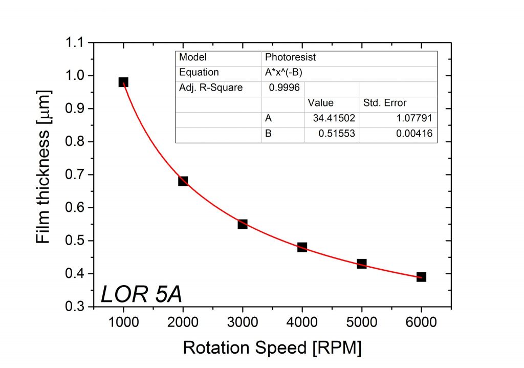


Available LOR thicknesses: 0.4 um / 0.7 um / 1.5 um
Coating:
| LOR thickness [μm] | Grade | Dispense method | Spin speed [RPM] | Spin duration [sec] | Notes |
|---|---|---|---|---|---|
| 0.4 | LOR 5A | dynamic, 1500RPM | 6000 | 25 | |
| 0.7 | LOR 5A | dynamic, 1500RPM | 1550 | 25 | |
| 1.5 | LOR 15C | ~static, 50RPM | 3200 | 30 |
Softbake:
| LOR thickness [μm] | Bake method | Temperature [°C] | Bake duration [sec] |
|---|---|---|---|
| 0.4 | proximity – 150um | 180 | 150 |
| 0.7 | proximity – 150um | 180 | 150 |
| 1.5 | proximity – 150um | 180 | 150 |
Available sequence options:
- Dehydrate / EBR
In order to maintain a clean wafer edge and backside, only EBR options are currently available after LOR coating.
- Find the spin-coating speed “XXXX” [RPM] matching your target thickness from both the LOR 5A, and LOR 15C spincurves.
- When coating on wafers, use the STD_”XXXX” recipe, which includes a 500 RPM spreading step and 40 seconds of main coating step.
- When coating on small chips, use the CHIP_”XXXX” recipe, which includes 60 seconds of main coating step and a short acceleration at the end to reduce edge bead effects.
- LOR 5A & LOR 15C cure temperature: 180°C
- LOR 5A & LOR 15C cure time: 4’10”
Imaging Resist
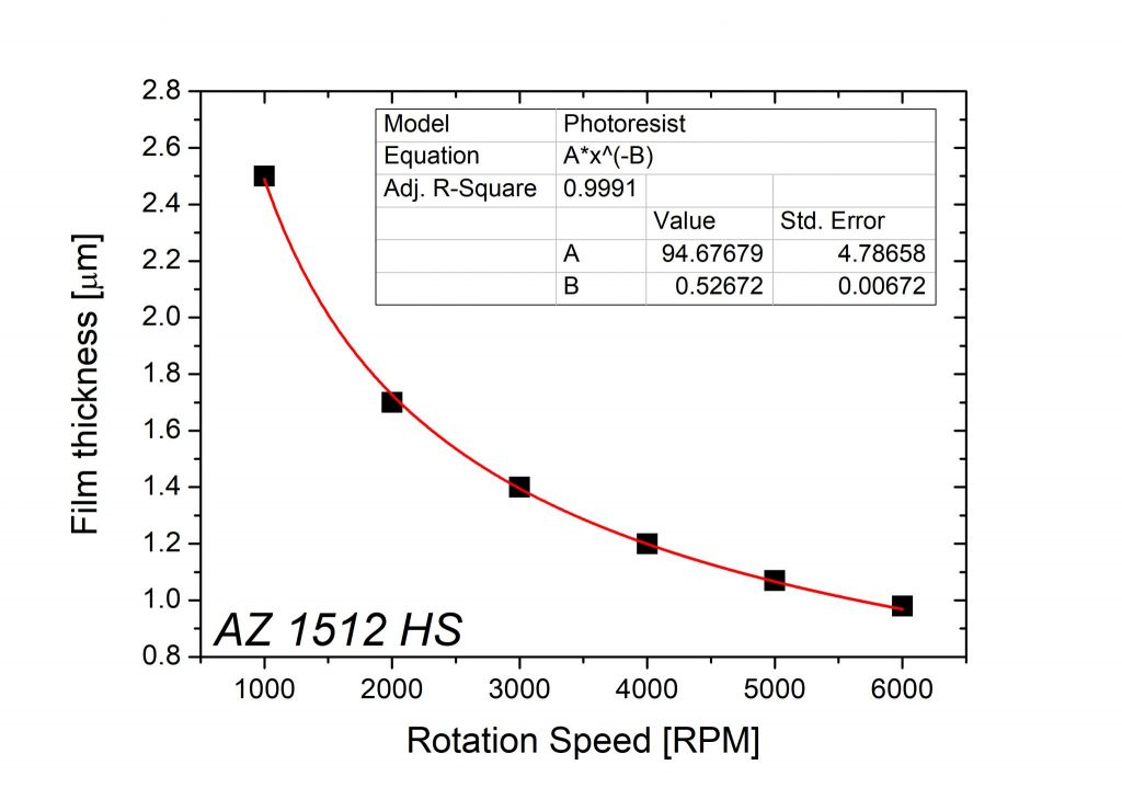
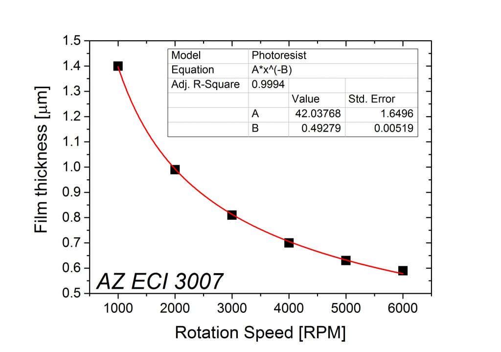
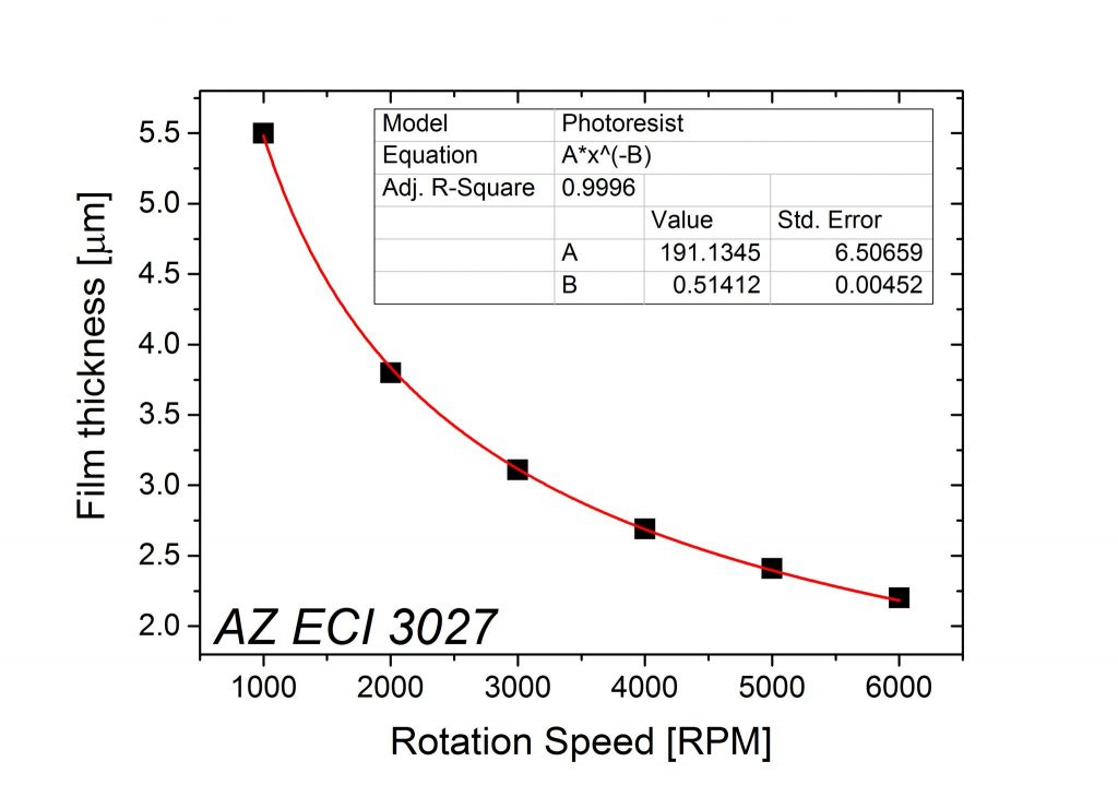
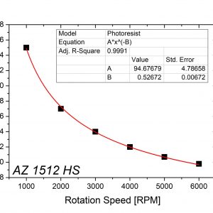
Users are free to coat any imaging resist on top of LOR layers but standard recommendations are AZ 1512 HS, AZ ECI 3007 or AZ ECI 3027, which are available on the EVG 150 automatic coater and the Sawatec SM-200 manual coater. The spincurves are shown below.


We recommend the following combinations:
| LOR thickness [μm] | Grade | PR thickness [μm] | Photoresist | Notes | |
|---|---|---|---|---|---|
| 0.4 | LOR 5A | + | 0.6 | AZ ECI 3007 | |
| 0.4 | LOR 5A | + | 1.1 | AZ 1512 HS | (from old EVG tool) |
| 0.7 | LOR 5A | + | 1 | AZ ECI 3007 | |
| 0.7 | LOR 5A | + | 1.5 | AZ 1512 HS | (from old EVG tool) |
| 1.5 | LOR 15C | + | 2.6 | AZ ECI 3027 |
The imaging resist is applied by spincoating directly after the LOR softbake, without any additional surface preparation.
On the EVG 150, make sure to select sequence without preparation, i.e. “C4.N.”…
On the Sawatec SM-200, make sure to use the correct spin-coating parameters for each photoresist.
Details are available here: AZ 1512 HS, AZ ECI 30XX
Exposure
The following table lists the typical exposure doses for some combinations of LOR and PR double layers, coated on silicon wafers.
Take note that your optimal dose depends on the layout type (isolated, dense lines & spaces, trenches, pillars, holes, etc…) and critical dimension (CD), as well as the wafer surface reflectivity. Please perform a dose series to determine the perfect match between the resulting pattern and the initial CAD layout dimensions.
| Illumination: | h-line (405 nm) | i-line (355-365 nm) |
|---|---|---|
| Equipment: | MLA 150, EVG 610 | MA6 Gen3 (filter), VPG200 |
| PR combination | Dose [mJ/cm2]+ | Dose [mJ/cm2]++ |
| LOR 5A 400nm + AZ1512 1.1um | 60 | 42 |
| LOR 5A 700nm + AZ1512 1.5um | 80 | 68 |
| LOR 5A 400nm + AZECI 3007 0.6um | 140 | 120 |
| LOR 5A 700nm + AZECI 3007 1.0um | 175 | 150 |
| LOR 15C 1.5um + AZECI 3027 2.6um | 280 | 250 |
+ Based on MLA150 internal dose measurements / ++ Based on intensity readings from Süss optometer i-line CCD
Development
The recommended developer for bilayers of LOR and imaging PR is AZ 726 MIF (or MF CD 26), an organic solution based upon TMAH. In general, the development duration is increased compared to the stand-alone photoresist process in order to create the LOR undercut. Dissolution rate of LOR is ~30nm/sec.
On the EVG 150, development of bilayers of LOR and imaging PR currently consists of running two sequences consecutively, which allows additional flexibility if one wants to optimize the LOR undercut: Sequence N°1 will develop the imaging PR and perform a stabilization bake (hardbake); Sequence N°2 will further etch the LOR layer to generate an undercut. By changing the sequence N°2, users can adjust the development time to create a smaller or larger undercut.
The recommended development routine consists in:
| PR combination |
Sequence N°1: PR development |
Sequence N°2: LOR undercut | |
|---|---|---|---|
| LOR 5A 400nm + AZ1512 1.1um | D4.1512.HB | + | D4.LOR.0u4-726MIF.15s |
| LOR 5A 700nm + AZ1512 1.5um | D4.1512.HB | + | D4.LOR.0u7-726MIF.30s |
| LOR 5A 400nm + AZECI 0.6um | D4.ECI3007.HB | + | D4.LOR.0u4-726MIF.15s |
| LOR 5A 700nm + AZECI 1.1um | D4.ECI3007.HB | + | D4.LOR.0u7-726MIF.30s |
| LOR 15C 1um5 + AZECI 2.6um | D4.ECI3027.HB | + | D4.LOR.1u5-726MIF.60s |
- Make sure to perform the PEB step if required (AZ ECI PR)!
- Recommended developer: AZ 726 MIF (no dilution needed)
- Development time: Use the standard development duration for the imaging resist (check details: AZ 1512 HS, AZ ECI) and add additional development time to create an undercut according to:
- LOR 5A, 400nm: + 15″ to the standard PR development time
- LOR 5A, 700nm: + 30″ to the standard PR development time
- LOR 15C, 1.5um: + 60″ to the standard PR development time
- Rinse: H2O 1min
IMPORTANT:
After development, it is mandatory for wafers to go through an additional rinsing step with DI water to avoid backside contamination and damage on equipments (chuck in etcher) in further processing steps. The water baths of the following wet benches can be used free of charge (5 min. billing delay after login):
- Z01 – Plade “Solvent” wet bench
- Z02 – UFT “Resist” wet bench
Pictures Gallery


