Master project
RTL-to-GDS flow for Superconducting Electronic Circuits

Description and contact info can be found here
Contact: Dr Gregor TAYLOR, [email protected]
Adaptive Digital Control and Self-Optimizing Calibration Architecture for Superconducting Qubit Systems
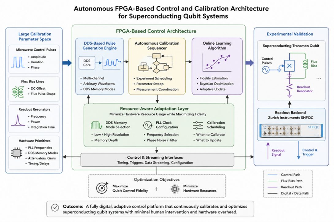
Description and contact info can be found here
Contact: Batuhan KESKIN, [email protected]
Enhancing Superconducting Detectors by Improved Fabrication Procedures – Characterisation

Description and contact info can be found here
Contact: Gregor TAYLOR, [email protected]
Cryogenic Transistor Model for CMOS Electronics Used in Quantum Applications
Description and contact info can be found here
Contact: Hung-Chi HAN, [email protected]
ML-based Parameter Extraction for Cryogenic Transistor Compact Models

Description and contact info can be found here
Contact: Hung-Chi HAN, [email protected]
GPU implementation of bi-exponential decay in FLIM for real time assistance in cancer cell localization
Description and contact info can be found here
Contact: Paul Mos, [email protected]
Towards real time monitoring of brain oxygenation for premature born infants
Description and contact info can be found here
Contact: Paul Mos, [email protected]
Towards real time monitoring of blood oxygenation in human body through Time Domain Diffuse Correlations Spectroscopy
Description and contact info can be found here
Contact: Paul Mos, [email protected]
System development of a real-time quantum distillation imager
Description and contact info can be found here.
Contact: Paul Mos, [email protected]
Test of a Photo Diode for the Swiss Light Source 2.0

Description and contact info can be found here
Contact: Rasmus Ischebeck, [email protected] Edoardo Charbon, [email protected]
RTL implementation for real time FLIM measurements
Description and contact info can be found here.
Contact: Paul Mos, [email protected]
Semester projects
Low-cost cryogenic infrastructure

Description and contact info can be found here
Contact: Gregor TAYLOR [email protected]
Mapping and scheduling Quantum Circuits on Distributed Cores with Logical Qubits

Description and contact info can be found here
Contact: Batuhan KESKIN [email protected]
ML-based Parameter Extraction for Cryogenic Transistor Compact Models
Description and contact info can be found here
Contact: Hung-Chi HAN [email protected];